

Patternable low dielectric constant materials and their use in ULSI interconnection
a dielectric constant and low-frequency technology, applied in the direction of photosensitive materials, semiconductor/solid-state device details, instruments, etc., can solve the problems of insufficient prior art multi-layer masking schemes of the type mentioned above, inefficient prior art process of patterning dielectric materials, and inability to efficiently route these signals across the device. to achieve the effect of reducing processing steps
- Summary
- Abstract
- Description
- Claims
- Application Information
AI Technical Summary
Benefits of technology
Problems solved by technology
Method used
Image

Examples
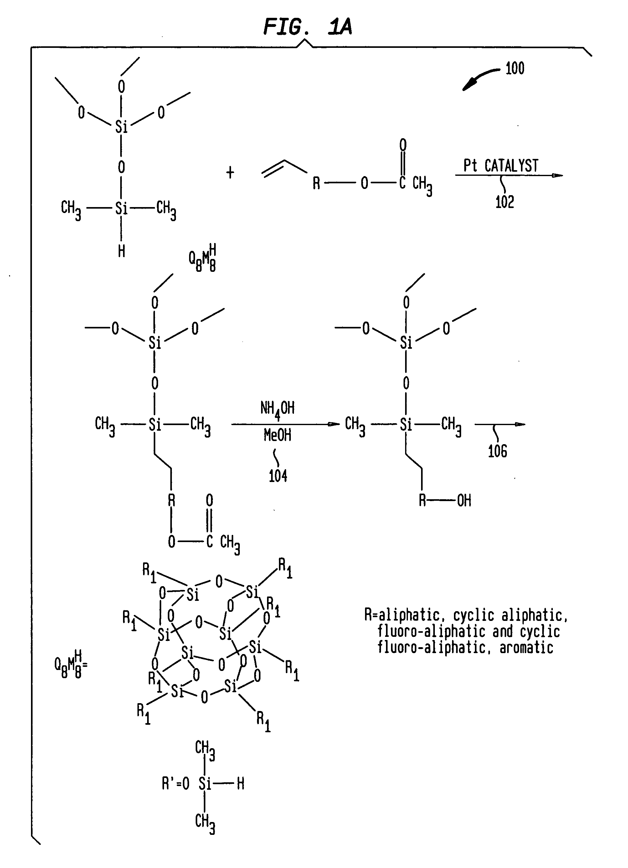
example 1
Synthesis of Octakis[(4-hydroxyphenethyl)dimethylsilyloxy]silsesquioxane (CSSQ HPE)
[0094]
Structure 1
[0095] I. Octakis(dimethylsilyloxy)silsesquioxane(Q8M8H) (10.16 grams, 0.01 mole), 4-acetoxystyrene(16.22 g, 0.1 mole) and hexane (100 ml) were placed in a round bottom flask equipped with magnetic stirrer, nitrogen inlet, and a water condenser. Platinum(0)-1,2-divinyl-1,1,3,3-tetramethyldisiloxane complex in xylene (1 ml) was added to this mixture and stirred at room temperature. The reaction became mildly exothermic. After half an hour at room temperature, the solution was heated to reflux for 2 hours. On cooling to room temperature, material separated and settled in the bottom as a waxy solid. This material was rinsed twice with hexane (30 ml) and dried under vacuum.
[0096] II. The above material was heated to reflux with methanol (100 ml) and ammonium hydroxide (14.8 molar) (12 ml, 0.18 mole) for two hours. The progress of the reaction was monitored by IR spectroscopy. The solu...
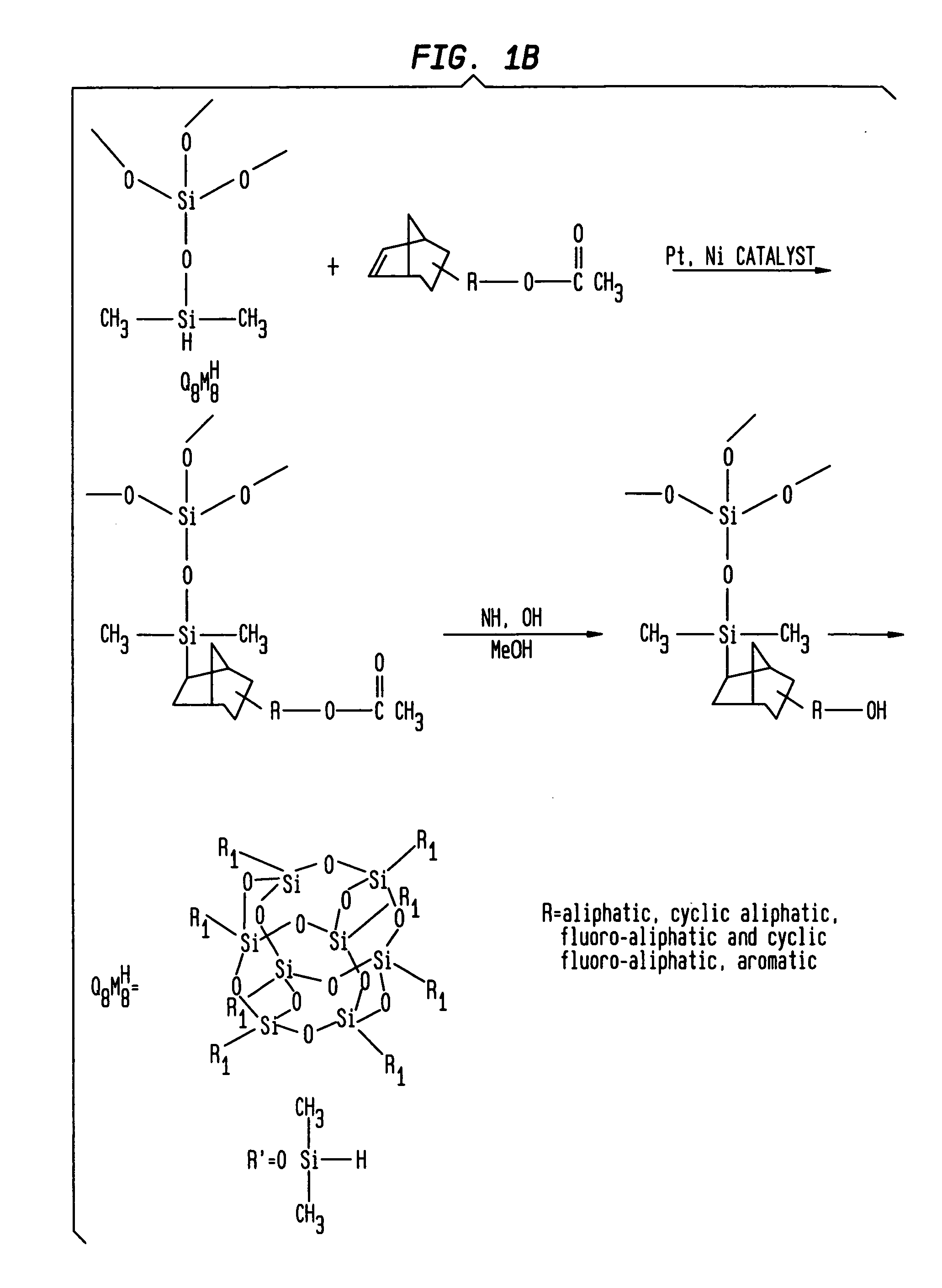
example 2
Synthesis of Octakis[{2-(1′, 1′-bis(trifluoromethyl)-1′-hydroxyethyl)norbornyl}dimethylsilyloxy]silsesquioxane (Structure 2) (CSSQ NBHFA)
[0099]
Structure 2
[0100] Using a similar procedure as in Example 1, 10.1 grams of Octakis[{2-(1′,1′-bis(trifluoromethyl)-1′-hyroxyethyl)norbornyl}dimethylsilyloxy]silsesquioxane (structure 2) was prepared from Octakis(dimethylsilyloxy)silsesquioxane (Q8M8H) (5.08 g, 0.005 mole) and 2-(1′,1′-bis(trifluoromethyl)-1′-acetoxyethyl)norbornene (14.2 g, 0.045 mole).
[0101] Notes: 2-(1′,1′-bis(trifluoromethyl)-1′-acetoxyethyl)norbornene was prepared from 2-(1′,1′-bis(trifluoromethyl)-1′-hydroxyethyl)norbornene (Central Glass, Japan), using a standard procedure (acetylchloride and triethyl amine).
example 3
Poly(4-hydroxy-α-methylbenzylsilsesquioxane) (PHMBS)
[0102] A patternable low-k composition was formulated with 1.0 g PHMBS, 0.33 g methylphenyltetramethoxymethyl glycoluril (methylphenyl POWDERLINK), 0.0925 g di(t-butylphenyl) iodonium triflate, 0.14 g of 1 wt. % coumarin-1 in propylene-glycolmonomethylether acetate (PGMEA), 0.067 g of 10% by weight surfactant (FLUORAD FC-430) in PGMEA, and 11.32 g propylene-glycolmonomethylether acetate (PGMEA) solvent. The resulting low-k formulation was filtered wafer and cured at 425° C. for 2 hours under N2 atmosphere. The resultant film had a dielectric constant as measured by MIS structure of 2.99 at 23° C. The dielectric constant, electrical breakdown field of the same film cured at 400° C. had a dielectric constant of 3.4, 5 MV / cm, respectively.
PUM
| Property | Measurement | Unit |
|---|---|---|
| dielectric constant | aaaaa | aaaaa |
| dielectric constant | aaaaa | aaaaa |
| Tg | aaaaa | aaaaa |
Abstract
Description
Claims
Application Information