Article comprising conductive conduit channels

a conduit channel and conductive technology, applied in the direction of dielectric characteristics, instruments, conductive pattern formation, etc., can solve the problems of insufficient other applications, insufficient size requirements for flexible circuits and rigid printed circuits, and insufficient size requirements for semiconductors and electrical connections between semiconductors and substrates, so as to reduce the height or z-direction thickness of the display, improve light transmission, and prevent shorting

Inactive Publication Date: 2006-05-25
EASTMAN KODAK CO
View PDF24 Cites 59 Cited by
  • Summary
  • Abstract
  • Description
  • Claims
  • Application Information

AI Technical Summary

Benefits of technology

[0015] The invention provides readily manufactured article exhibiting improved light transmission while simultaneously providing conductive conduits. The invention also provides protection for the delicate conductive coatings from abrasion or harsh ambient conditions such as those typical of display devices. When used to make displays and TFT's, this invention serves to reduce the height or Z-directional thickness of the display. In areas where there are electrical crossovers of two or more electrically conductive features as well as a way of providing electrical isolation to prevent shorting between the electrical conducting features, the thickness of these layers and any transition areas approaching or leaving the crossover region use a large amount of area and that can interfere with the viewing of the display pixels. Typically conductive lines used for flexible displays are very thin and brittle and are prone to breakage when flexed or are subjected to abrasion that can break the electrical continuity of the conductive line and render the article or parts of it useless. By providing conductive lines that are below the surface of the polymer sheet (substrate), many of these problems can be overcome because they are not in direct contact with the physical environment at the surface such as a viewer touching or otherwise handling the display. Furthermore if multiple layers of conductive material and dielectrics are placed in a trench, the surface is free of conductive lines and may be processed in a roll-to-roll manufacture process without fear of damaging the display. Also by burying the conductive lines, crossover regions can be made without added height to the display plane that otherwise will result in optical viewing problems. By placing the electrically conductive electrodes closer to the central axis of the flexible, any bending in either compression or expansion will be more uniform and therefore provide for a more robust display.

Problems solved by technology

As electronic appliances, such as computers, tape players, televisions, telephones, and other appliances become smaller, thinner, and more portable, the size requirements for semiconductors and the electrical connections between semiconductors and substrates, or between flexible circuits and rigid printed circuits, become increasingly demanding.
Whether the sheet material is elastomeric or adhesive, the continuing challenge is to keep pace with the miniaturization in the electronics industry.
The distribution of the particles after orientation and curing is sufficiently uniform to be functional for certain applications, but is insufficient for other applications.
If the number of particles used in these articles were to be increased in an attempt to reach smaller spacings for finer pitch connections, agglomeration would likely occur thereby causing shorting.
While conductive materials are disclosed, they tend to have low light transmission and therefore are not particularly useful in transmission devices such as liquid crystal displays.
The engraving process has many limitations including misalignment causing tool lines in the surface, high price, and lengthy processing.
This method is difficult to apply to create a master chill roll useful to manufacture complex random three-dimensional structures and is also cost prohibitive.
Processing steps to apply and then remove parts of the stage layer leave the electrode structures prone to damage from handling and conveyance.
Additionally the structures described are difficult to make because they are coated and then patterned to form regions of different heights.
Subtractive removing of material is always more costly and difficult to control particularly when the feature size being made is in the micron range.
Overall this is a very complicated process and design and there remains a need to protect the electrodes and dielectric layer from damage while providing a process that is more simple and less costly.

Method used


Image

  • Article comprising conductive conduit channels
  • Article comprising conductive conduit channels
  • Article comprising conductive conduit channels

Examples


examples

[0155] In this example, polycarbonate V shaped conduits were formed integral to a polycarbonate 100 micrometer sheet. A conductive, transparent form of polythiophene was applied into the V shaped conduits creating a transparent conductive sheet. This invention will demonstrate the conductive and transmissive properties of the polymer sheet containing the conductive, transparent polymer.

[0156] The V shaped conduits were made by casting melted polcarbonate against a heated roller containing the negative of the V groove pattern. The V-groove patterned roller was manufactured by precision machining, utilizing a wire EDM cutting tool, the negative of the V groove pattern into the surface of a smooth steel roller.

[0157] The V groove patterned roller was used to create the integral polycarbonate conduits by extrusion casting a polycarbonate polymer from a coat hanger slot die comprising substantially 98.0% 68 melt index CD grade polycarbonate (Bayer Chemical), 1.5% antioxidant and 0.5% r...

example 2

This Example is Both in Past and Present Tense, Revise

[0164] An electromodulating display cell was formed by extrusion roll molding a V-groove pattern in a sheet of polycarbonate as describe in the above example. The V-groove was further made conductive as per the above example. The sample was then spun coated with an organic resin solution that was a negative photo-resist. It should be noted that an area of the V-groove needs to be left uncoated on at least 2 sides for electrical connections. This is needed so the electrode formed by the V-groove with the conductive material can be switch from positive to negative or off. The material is SU-8 2010 series (Y111058) manufactured by MicroChem. A layer of approximately 10 micron is spun coated at 3000 PRM.

[0165] The sample is prebaked for approximately 3 minutes at an elevated temperature of approximately 65° C. A photo mask is prepared separately using Kodak Direct Image Setting Film (available from Eastman Kodak Company) and laser...

example 3

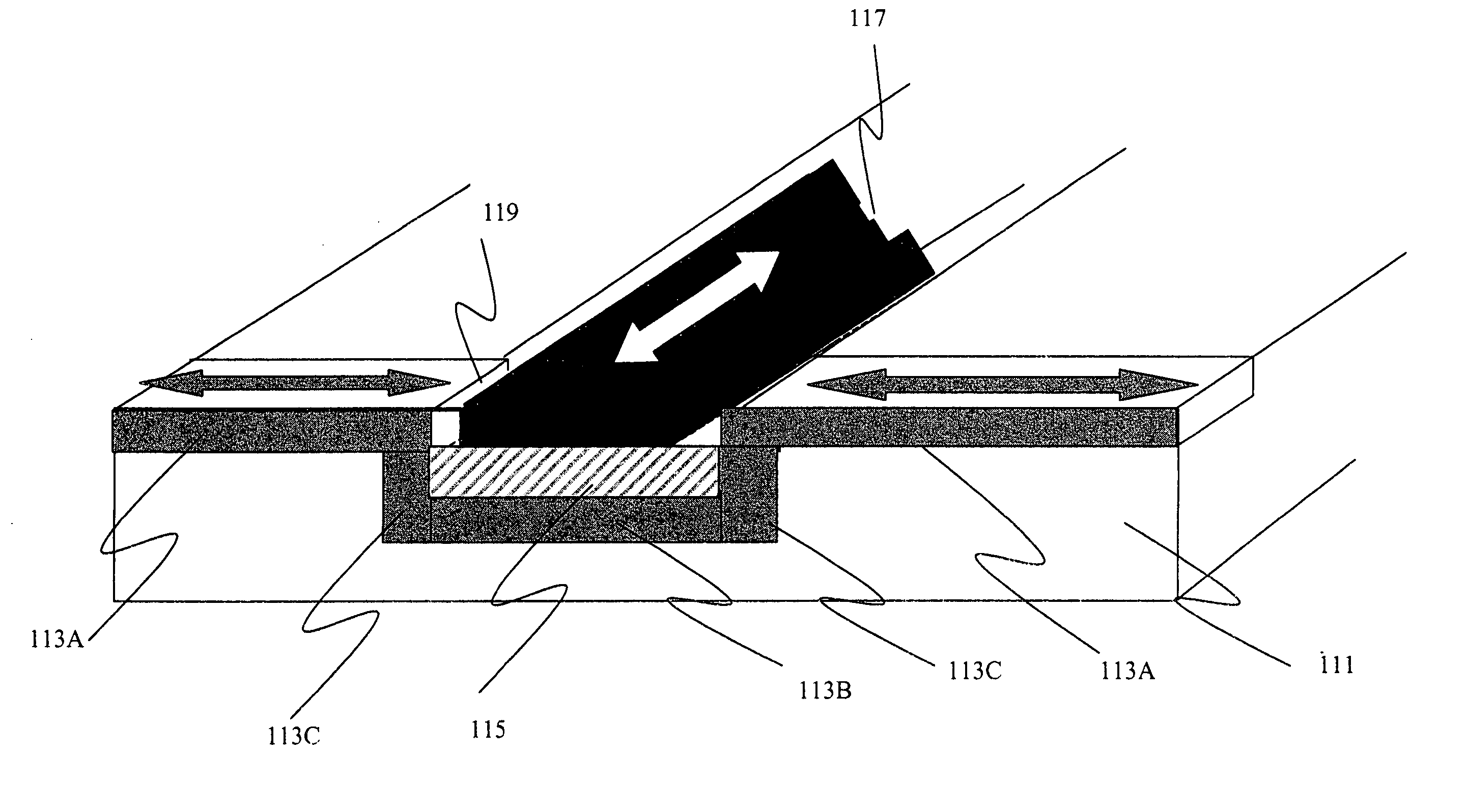
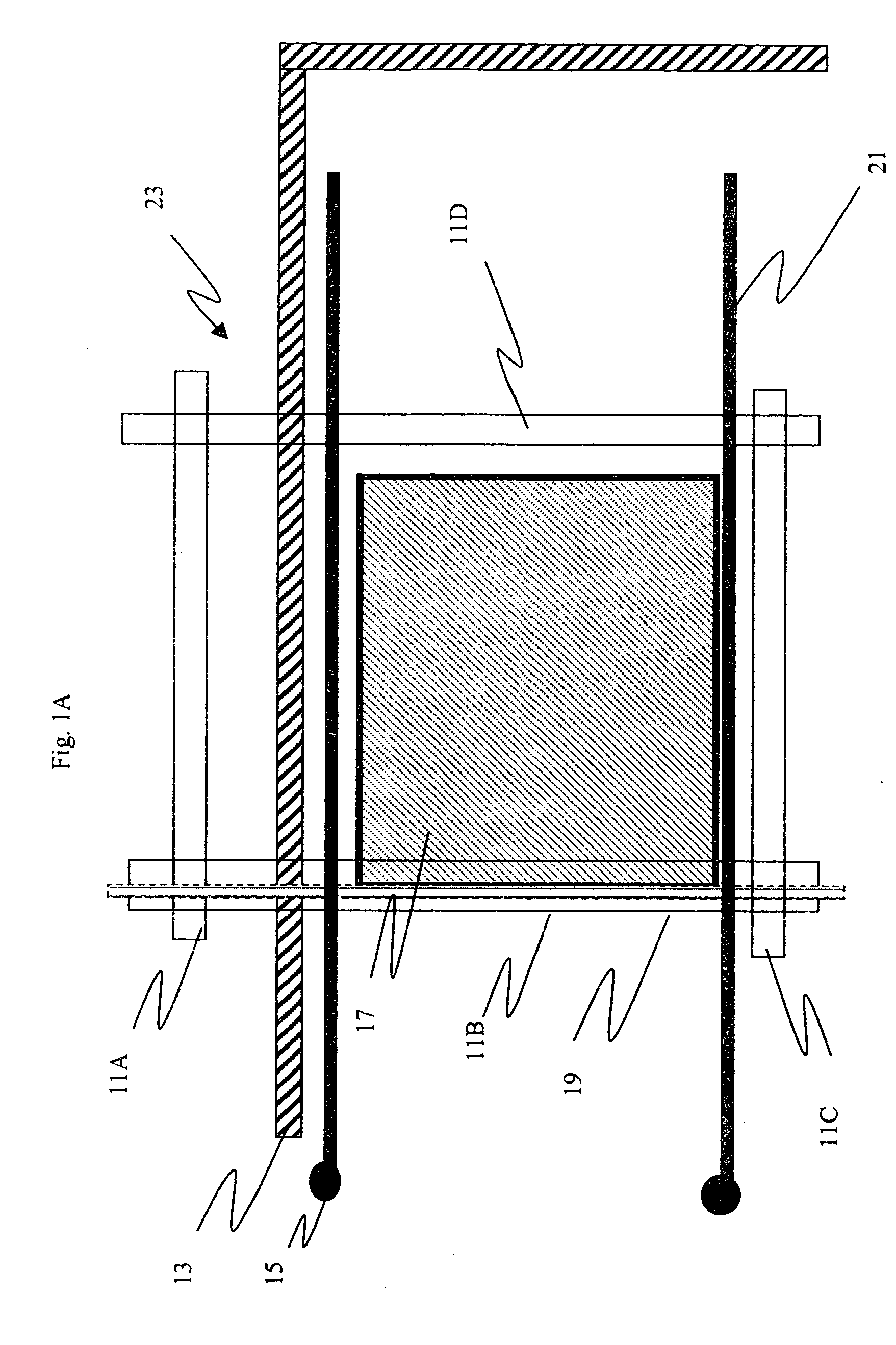
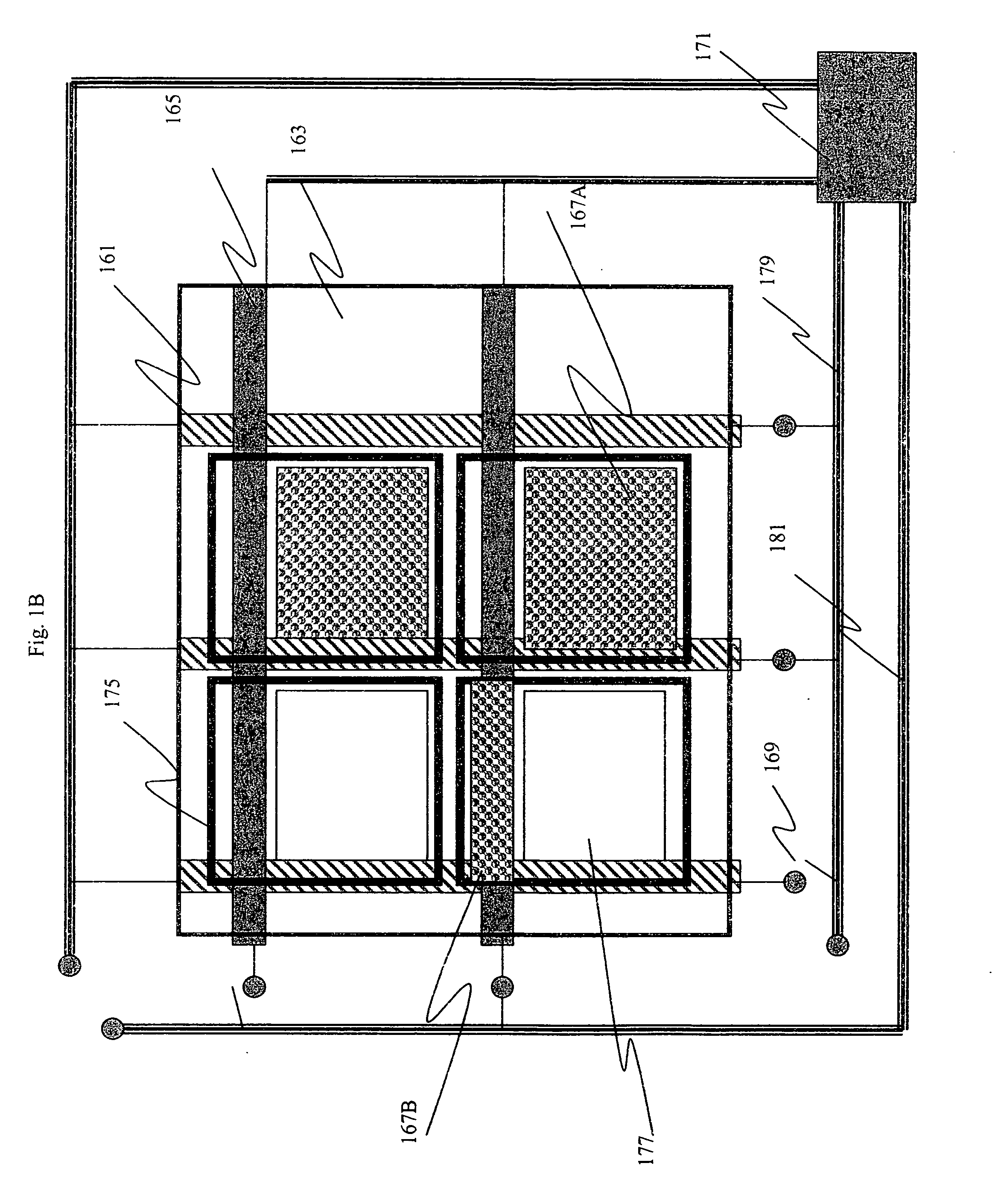
[0168] This example is another electromodulating display. A polycarbonate sheet with multiple pixels is prepared to look like FIG. 6. A polycarbonate sheet is grooved to form a trenches in the polymer sheet 121 that correspond to flag electrode bus-bar 123A that feeds flag electrode 125, collector electrode bus-bar 127 that feeds collector electrode 129, gate electrode bus-bar 131 that feeds gate electrode 135 and helper bus-bar electrode 137 that feeds helper electrode 139. The V-groove trenches formed are approximately 10 to 15 microns deep. The flag electrode bus-bars trenches (123A), gate bus-bar electrode trenches 131, collector electrode bus-bar trenches 127 and helper bus-bar electrode trenches 137 is patterned coated with a nano gold particle with a mean particle of approximately 5 nm. The gold particles were than sintered with a laser to form a continuous network of conducting metal in the trenches. The metal thickness in the trenches is less than 5 microns in thickness. A ...


PUM

PropertyMeasurementUnit
diameteraaaaaaaaaa
reflectanceaaaaaaaaaa

Abstract

An electromodulating display comprises (1) a nonconductive polymeric unitary substrate containing a plurality of patterned grooves containing an electrically-conductive material so as to form an electrical network having a switchable electric field orientation; (2) a switch for switching the electric field orientation; and (3) a medium that is optically shifted in response to the switching of the electric field orientation.

Description

CROSS REFERENCE TO RELATED APPLICATIONS [0001] This application is a continuation-in-part of U.S. Ser. No. 10 / 425,005 filed Apr. 28, 2003, the contents of which are incorporated herein by reference. Inventions on related subject matter are disclosed in U.S. Ser. Nos. 10 / 424,666; 10 / 424,639; and 10 / 425,012, all filed on Apr. 28, 2003.FIELD OF THE INVENTION [0002] The invention relates to an article comprising a patterned conductive sheet aligned to form conduits in the plane of the conductive sheet. BACKGROUND OF THE INVENTION [0003] As electronic devices become smaller, the requirements for precise electrical connection at extremely fine pitch continue to increase. As an example, semiconductors, such as integrated circuits, are formed on silicon wafers that are then cut into dice or chips that individually may be mounted on substrates. Typically, the substrate has fine electrically conductive circuit lines, and electrical and thermal contact must be made between the substrate and ch...

Claims


Application Information

Patent Timeline
Patent Type & Authority Applications(United States)
IPC IPC(8): B32B3/00H05K1/02H05K3/10H05K3/28
CPCG02B26/004G02F1/133305G02F1/136286G02F2001/13629G02F2001/136295H05K1/0274Y10T428/24612H05K3/28H05K2201/0108H05K2201/0329H05K2201/09036H05K2203/161H05K3/107G02F1/13629G02F1/136295
Inventor AYLWARD, PETER T.KAMINSKY, CHERYL J.BOURDELAIS, ROBERT P.CROSDALE, FITZROY H.MAJUMDAR, DEBASISSLATER, DANIEL A.
Owner EASTMAN KODAK CO
Why Eureka
Try Eureka