

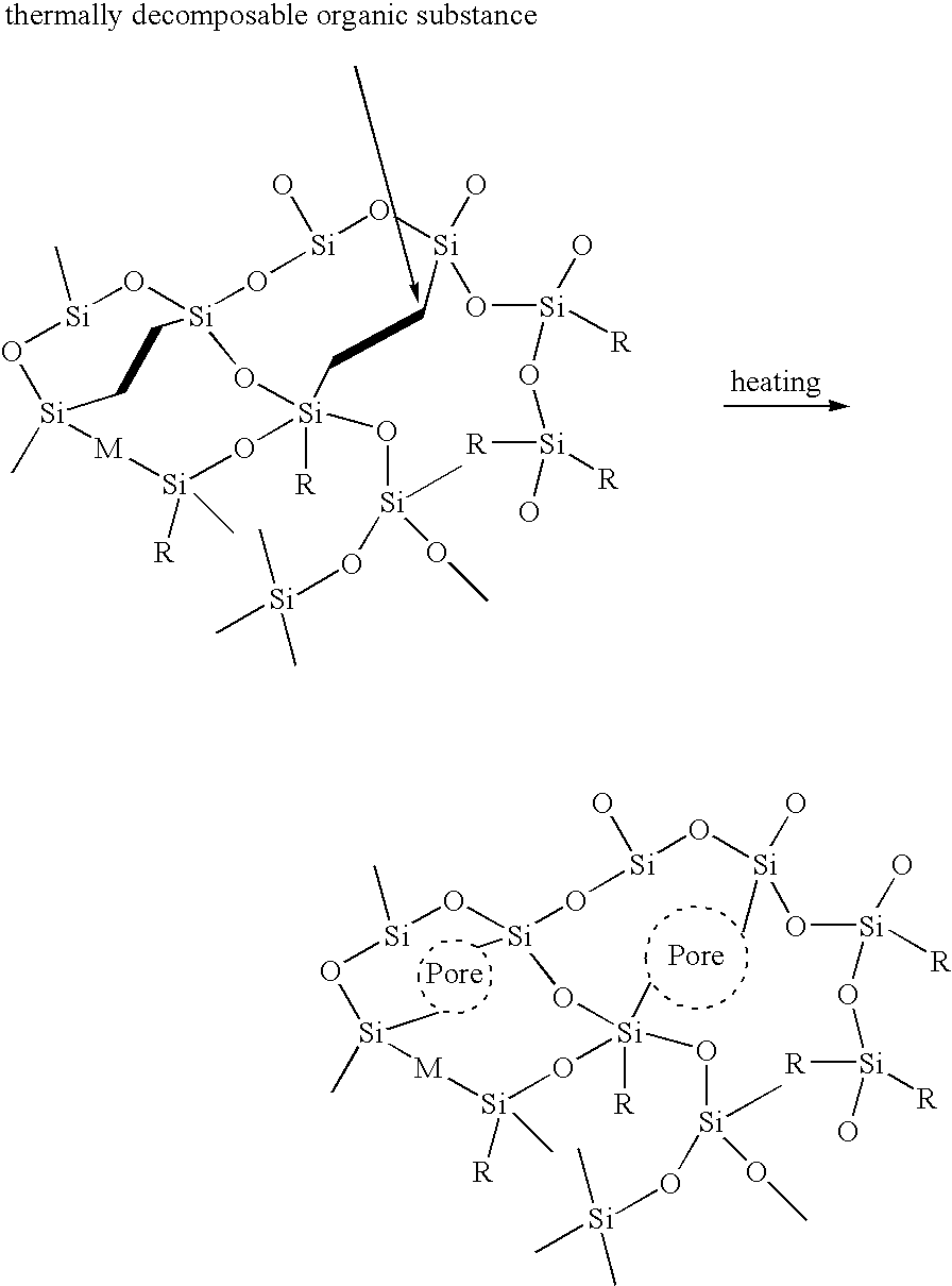
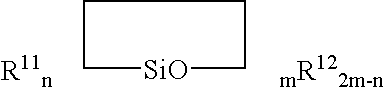
Organic silicate polymer and insulation film comprising the same
a technology of organic silicate polymer and insulation film, which is applied in the direction of organic chemistry, semiconductor/solid-state device details, coatings, etc., can solve the problems of difficult to commercialize a semiconductor device using a low dielectric material, low glass transition temperature, and difficult to lower the dielectric constant below 3.5. , to achieve the effect of reducing cross-talk between metal wiring, high speed and low cos
- Summary
- Abstract
- Description
- Claims
- Application Information
AI Technical Summary
Benefits of technology
Problems solved by technology
Method used
Image


Examples
example 1
[0078] To a 250 mL round-bottom flask, 16 g of methyltrimethoxysilane and 7.16 g of tetramethoxy silane were dissolved in 24 g of propyleneglycol methylether acetate, and then 19.46 g of distilled water in which 514 mg of malonic acid was dissolved was added thereto while stirring with a stirrer. The temperature of the reactor was elevated to 60° C. and the reaction solution was reacted for 3 hours. Then the temperature was lowered to room temperature, and 2.08 g of distilled water and 6.4 g of propyleneglycol methylether acetate in which 4.26 g of bismethyldimethoxysilylpropyl polypropyleneoxide was dissolved were added. Then, the temperature of the solution was elevated to 60° C., the reaction solution was reacted for 20 hours, and then the temperature of the solution was lowered to room temperature. 70 g of propyleneglycol methylether acetate was added thereto, and 70 g of solvent comprising methylalcohol was evaporated from the reaction solution to obtain a coating composition f...
example 2
[0079] A coating composition for forming an insulating film was obtained by the same method as in Examples 1, except that bistrimethoxysilylpropyl (polyethyleneoxide-b-polypropyleneoxide-b-polyethyleneoxide) was used instead of bismethyldimethoxysilylpropyl polypropyleneoxide.
example 3
[0080] A coating composition for forming an insulating film was obtained by the same method as in Examples 1, except that 3.72 g of distilled water and 11.4 g of a propyleneglycol methylether acetate solution in which 7.60 g of bismethyldimethoxysilylpropyl polypropyleneoxide was dissolved were further added, the temperature of the solution was elevated to 60° C., and the reaction solution was reacted for 20 hours, and then 80 g of propyleneglycol methylether acetate was added thereto, and 80 g of solvent comprising methylalcohol was evaporated from the reaction solution.
PUM
| Property | Measurement | Unit |
|---|---|---|
| Temperature | aaaaa | aaaaa |
| aaaaa | aaaaa |
Abstract
Description
Claims
Application Information