Method of making a semiconductor chip assembly using multiple etch steps to form a pillar after forming a routing line
a technology of semiconductor chips and routing lines, applied in semiconductor devices, semiconductor/solid-state device details, electrical devices, etc., can solve the problems of significant cost and technical limitations, over-all cost saving, and significant cost of forming bumps on pads, etc., to improve uniformity, facilitate manufacturing, and enhance mechanical support and protection
- Summary
- Abstract
- Description
- Claims
- Application Information
AI Technical Summary
Benefits of technology
Problems solved by technology
Method used
Image

Examples
Embodiment Construction
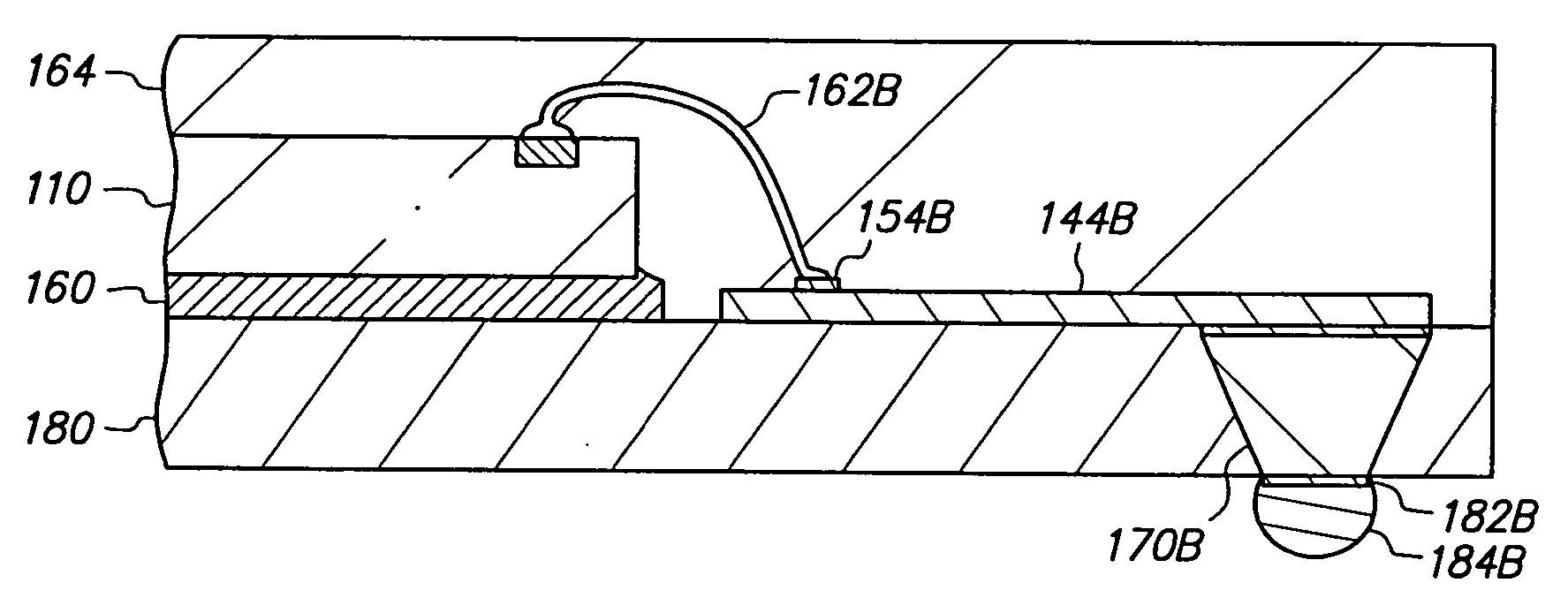
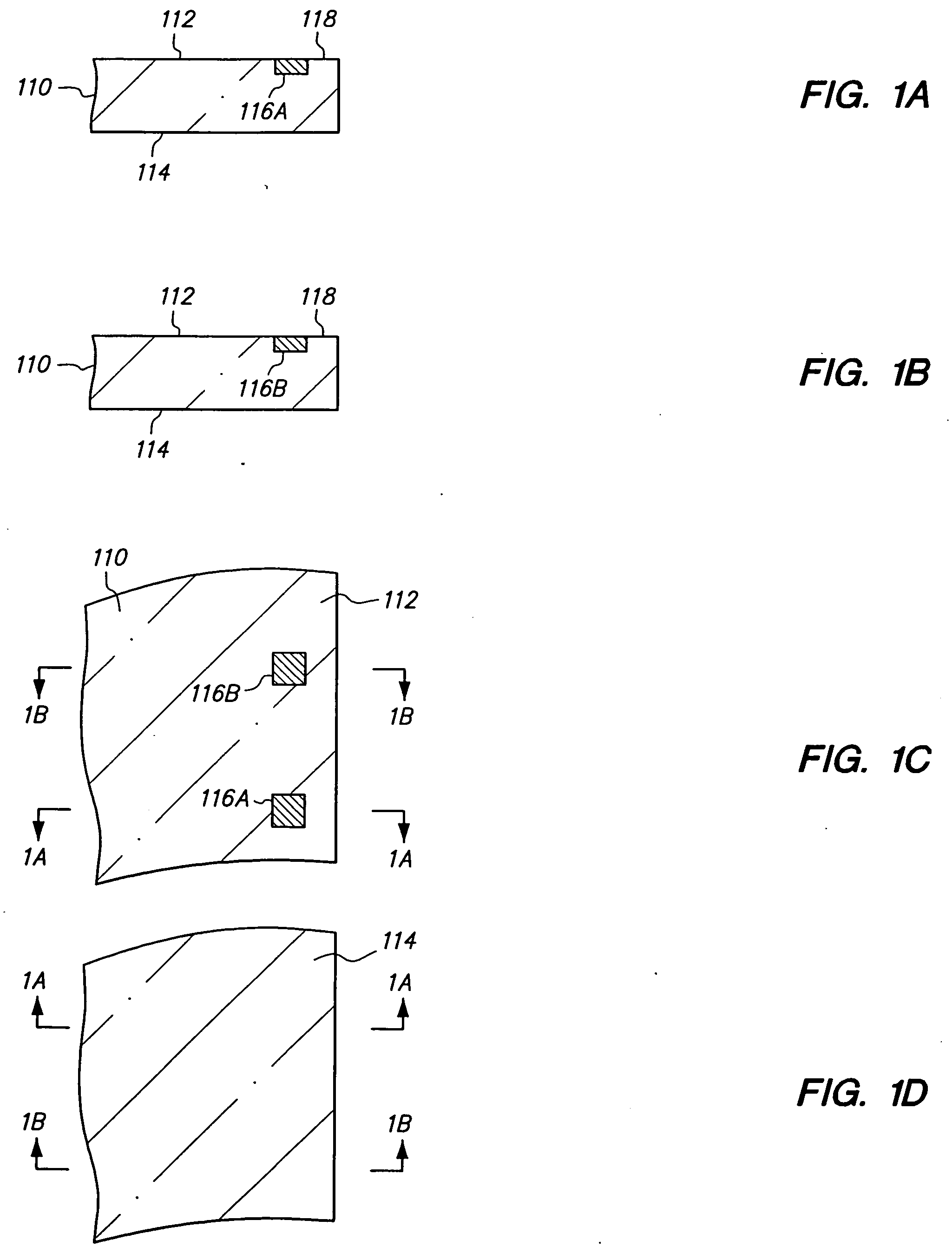
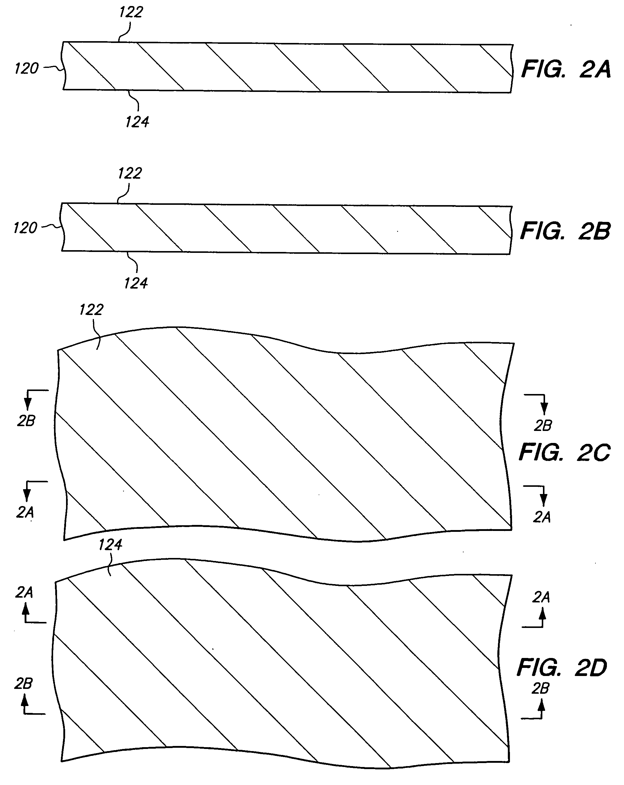
[0069]FIGS. 1A-22A, 1B-22B, 1C-22C and 1D-22D are cross-sectional, cross-sectional, top and bottom views, respectively, of a method of making a semiconductor chip assembly in accordance with an embodiment of the present invention.
[0070]FIGS. 1A, 1B, IC and 1D are cross-sectional, cross-sectional, top and bottom views, respectively, of semiconductor chip 110 which is an integrated circuit in which various transistors, circuits, interconnect lines and the like are formed (not shown). Chip 110 includes opposing major surfaces 112 and 114 and has a thickness (between surfaces 112 and 114) of 150 microns. Surface 112 is the active surface and includes conductive pads 116A and 116B and passivation layer 118. Pads 116A and 116B provide bonding sites to electrically couple chip 110 with external circuitry.
[0071] Pads 116A and 116B are substantially aligned with passivation layer 118 so that surface 112 is essentially flat. Alternatively, pads 116A and 116B can extend above or be recessed ...
PUM
 Abstract
Description
Claims
Application Information