Charge trapping semiconductor memory element with improved trapping dielectric

a charge-trapping semiconductor and memory element technology, applied in the direction of semiconductors, electrical devices, transistors, etc., can solve the problems of unsatisfactory data retention, restricted data retention, and increased leakage current, and achieve the effect of improving data retention and charge-trapping memory cell efficiency, and allowing further miniaturization of charge-trapped memory cells

Active Publication Date: 2006-09-07
INFINEON TECH AG
View PDF5 Cites 16 Cited by
  • Summary
  • Abstract
  • Description
  • Claims
  • Application Information

AI Technical Summary

Benefits of technology

[0011] In accordance with the present invention, a semiconductor memory element, that is controllable via field effect, comprises a trapping dielectric, which has improved data retention and charge carrier trapping efficiency as compared to conventional semiconductor memory elements with trapping dielectrics, and is suitable for allowing further miniaturization of charge trapping memory cells.
[0013] In this context, it is important that, in the layer sequence comprising an amorphous silicon carbide layer and an amorphous silicon nitride layer, the layers are adjacent to one another, thus forming a layer junction. It is in this way possible to greatly increase the density of deep impurities beyond the deep impurities which are already present in the bulk of the two layers, due to the network mismatch of the amorphous silicon carbide layer and the amorphous silicon nitride layer, and the additional deep impurities which are introduced as a result in the boundary region between the two layers. More specifically, what are known as dangling bonds, i.e., open, unsaturated silicon bonding sites or torn-off silicon bonds, which occur on account of the inadequate network matching, are produced at the interface between the two amorphous networks of the amorphous silicon carbide layer and the amorphous silicon nitride layer. On account of the thermal stability of silicon carbide, these deep impurities cannot be annealed in the mobility gap, which corresponds to the term “band gap” for amorphous materials. The stability of the amorphous silicon carbide network also has a positive influence on the stability of the charge storage in the deep impurities.
[0014] According to the invention, therefore, the density of deep impurities in the mobility gap between the valence band and conduction band of the charge trapping memory layer can be increased in an extremely advantageous way. With the sequence comprising a silicon carbide layer and a silicon nitride layer, producing the increased density of the deep impurities, which are additionally present in the bulk, it is possible to produce densities of deep impurities in the range of 3×1019 cm−3 in the charge trapping memory layer. It is in this way possible to considerably increase the data retention and efficiency of charge trapping as compared to conventional charge trapping memory elements. In this context, amorphous silicon carbide layers, on account of their electrical properties such as: leakage currents in the region of 10−13 A, electrical resistivity of up to 1015 ohmcm and dielectric strength in the region of 5×10⁶ V / cm, are suitable for use as charge trapping memory layers, especially in combination with a silicon nitride layers. The thermal stability of the amorphous silicon carbide layer, which only begins to recrystallize into beta-silicon carbide at relatively high thermal stresses, e.g., 900° C. for a period of 3 hours, has proven particularly advantageous in this context. On account of the stability of the amorphous silicon carbide network, it is to be expected that the data retention in the deep impurities will also be improved, since relatively high thermal energies are required to reorganize the network and / or saturate the deep impurities generated at the interface.
[0018] In a further preferred embodiment of the memory element, the amorphous silicon carbide layer within the layer sequence is arranged on the substrate side. The mobility gap, i.e., band gap, of the amorphous silicon carbide, in the case of virtually stoichiometric silicon carbide, is approx. 3.2 to 3.5 eV, and is therefore lower than the mobility gap, i.e., band gap, of the amorphous silicon nitride (Si3N4 or SiN), which is approx. 4.5 eV. Therefore, since the amorphous silicon carbide layer is arranged on the substrate side, it is possible to advantageously increase the trapping probability for the charge carrier injection into the charge carrier memory layer.

Problems solved by technology

However, specifically capacitive coupling of this type constitutes a serious problem in the context of ongoing miniaturization, and this problem is the subject of intensive research in the field of memory cells with a floating gate, in particular in the form of multilevel transistors, as what is known as floating gate / floating gate interference.
In this regard where the charge carriers have to be trapped in deep impurities, the Si3N4 / SiN layer, which is customarily used for the memory layer, presents a problem, with regard to the desire to constantly reduce the minimum feature size, since it has a relatively small number of deep impurities and a relatively low efficiency in terms of trapping charge carriers and therefore, it possess restricted data retention.
However, this approach leaves open the question as to whether the Si-richer phases actually generate further deep impurities, since these phases can also lead to Si—Si bonds.
Furthermore, this Si-richer phase can lead to an increase in the leakage current.
In addition, the data retention achieved by this method is unsatisfactory.

Method used


Image

  • Charge trapping semiconductor memory element with improved trapping dielectric
  • Charge trapping semiconductor memory element with improved trapping dielectric
  • Charge trapping semiconductor memory element with improved trapping dielectric

Examples


Embodiment Construction

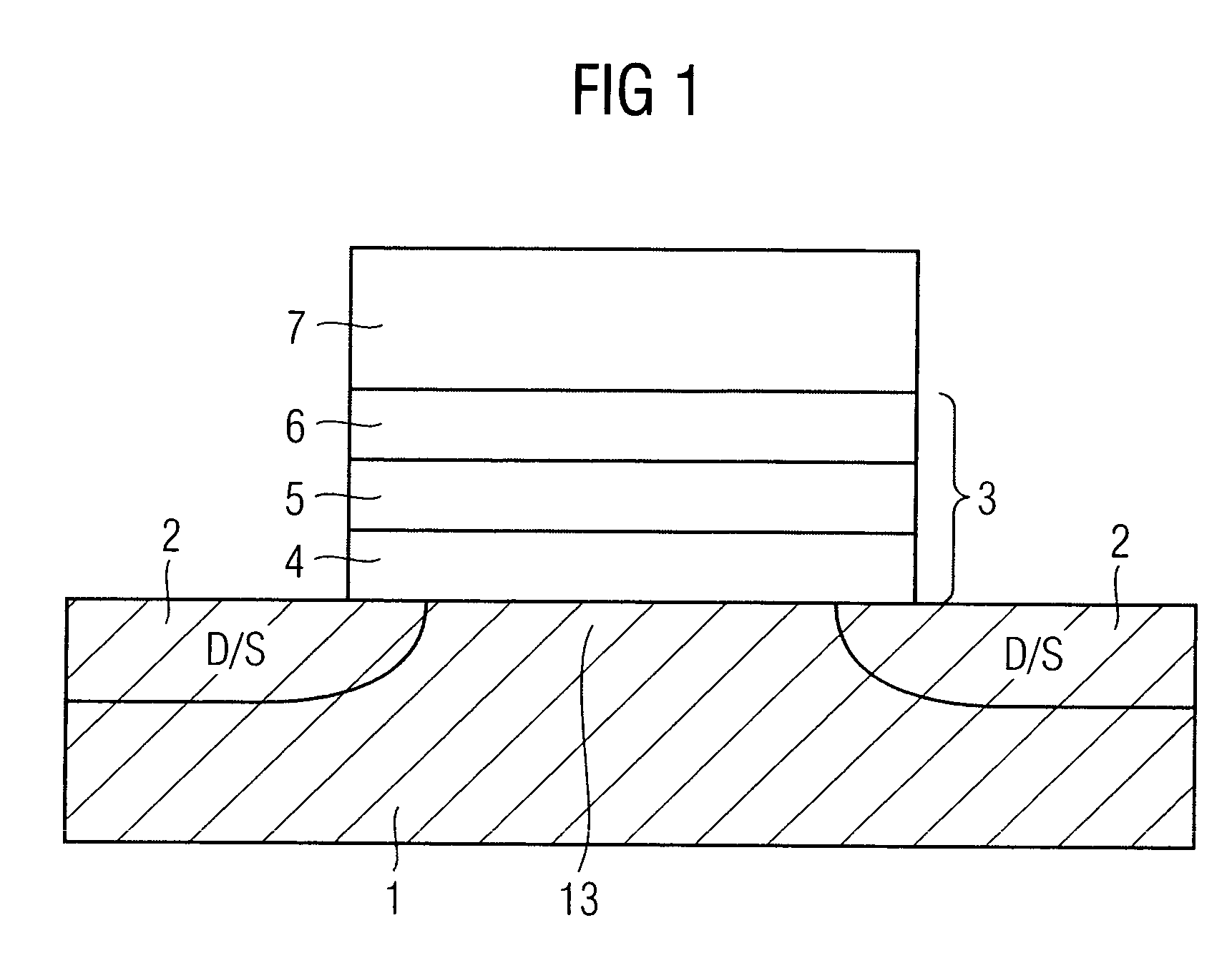
[0026]FIG. 1, shows a vertical section through a conventional semiconductor memory element of an SONOS flash memory structure in planar geometry. Accordingly, in a p-doped silicon substrate n-doped source / drain regions are formed at a surface of the silicon substrate. Between the n-doped source / drain regions there is a channel region. Above the channel region is a multilayer gate dielectric in the form of a layer stack. The gate dielectric consists of a first oxide layer, which is a tunneling layer, a nitride memory layer for trapping charge carriers from the substrate and a second oxide layer. Above the second oxide layer there is a gate terminal, which comprises a polysilicon gate. The polysilicon gate is generally connected to a gate supply voltage, while at the same time the substrate is grounded.

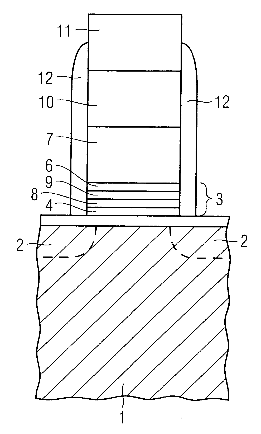
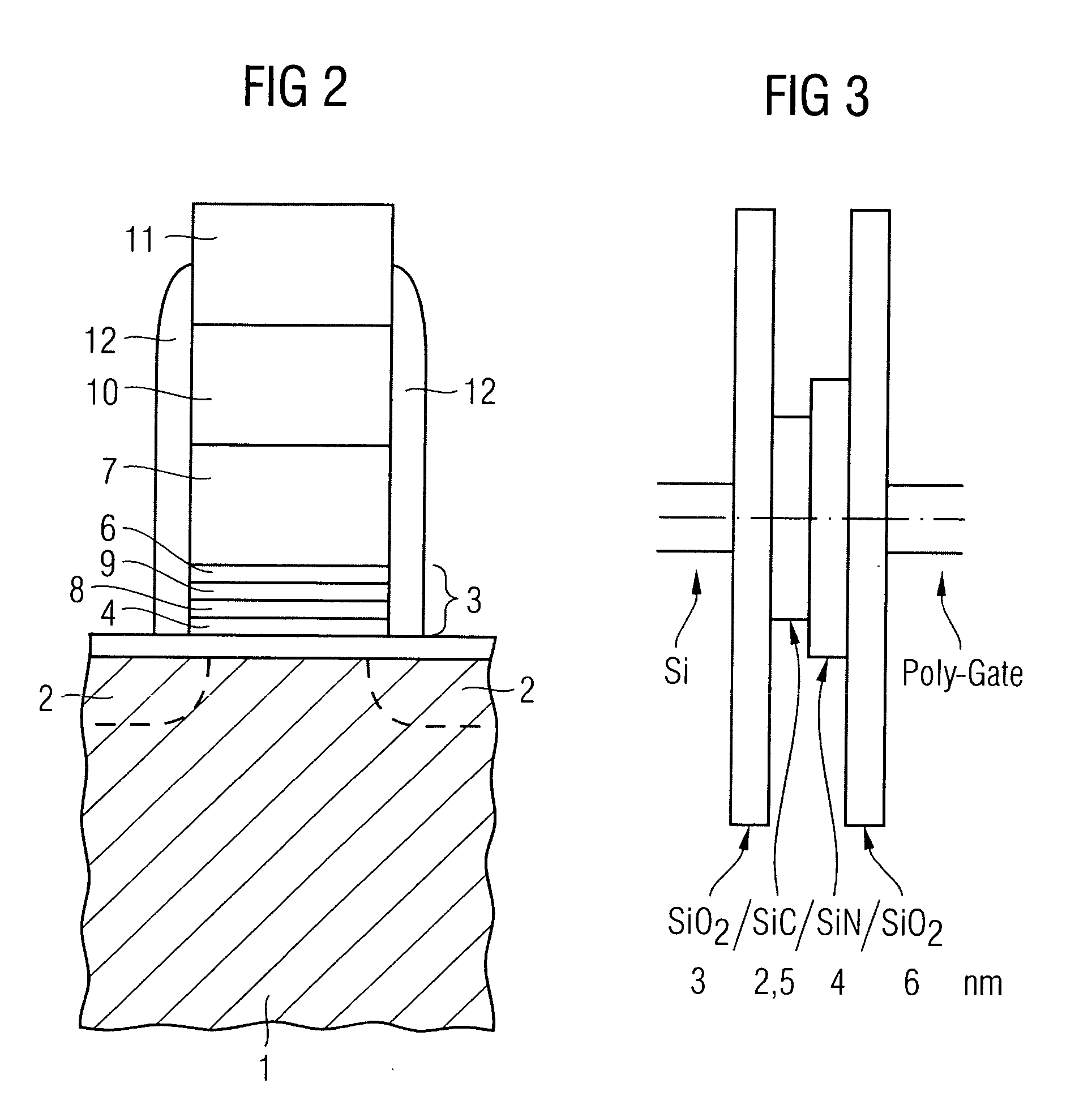
[0027]FIG. 2, shows a vertical section through a semiconductor memory element according to the invention, wherein the gate dielectric has a quadruple layer structure. To avoid unnecess...


PUM


Abstract

A semiconductor memory element, which can be controlled via field effect, includes a semiconductor substrate of a first conduction type, a first doping region of a second conduction type provided in the semiconductor substrate, a second doping region of the second conduction type provided in the semiconductor substrate, a channel region located between the first and second doping regions, a multilayer gate dielectric which is arranged adjacent to the channel region and has a charge trapping memory layer, and a gate terminal provided above the gate dielectric. The charge trapping memory layer includes at least one sequence of adjacent layers, wherein the sequence of adjacent layers comprises an amorphous silicon carbide layer and an amorphous silicon nitride layer.

Description

CROSS REFERENCE TO RELATED APPLICATIONS [0001] This application claims priority under 35 USC §119 to German Application No. DE 10 2005 008 321.8, filed on Feb. 23, 2005, and titled “Charge Trapping Semiconductor Memory Element with Improved Trapping Dielectric,” the entire contents of which are hereby incorporated by reference. FIELD OF THE INVENTION [0002] The present invention takes effect within the technical field of electrically writable and erasable, nonvolatile semiconductor memories and relates in particular to a charge trapping semiconductor memory element which can be controlled by means of field effect and has a multilayer gate dielectric for trapping charge carriers. BACKGROUND [0003] A semiconductor memory cell, which is based on the principle of charge trapping, has a memory transistor, which is positioned on a top side of a semiconductor body (substrate) or of a semiconductor layer, which is provided with a gate electrode arranged between the source and drain regions ...

Claims


Application Information

Patent Timeline
Patent Type & Authority Applications(United States)
IPC IPC(8): H01L29/788H01L21/8238
CPCH01L21/28282H01L27/115H01L27/11568H01L29/513H01L29/792H01L29/40117H10B69/00H10B43/30
Inventor UFERT, KLAUS-DIETERWILLER, JOSEF
Owner INFINEON TECH AG
Why Eureka
Try Eureka