Light emitting device

a light emitting device and light technology, applied in semiconductor lasers, instruments, applications, etc., can solve the problems of shortened life of light emitting devices, hot and fluorescent materials, and deformation of wavelength converting members, so as to prevent the degradation of members and good light emitting efficiency

Active Publication Date: 2006-09-07
NICHIA CORP
View PDF2 Cites 41 Cited by
  • Summary
  • Abstract
  • Description
  • Claims
  • Application Information

AI Technical Summary

Benefits of technology

[0011] An object of the present invention is to provide a long-lasting light emitting device which uses semiconductor light emitt

Problems solved by technology

However, the light density of semiconductor light emitting elements is extremely high, so the resin and fluorescent material or the like which make up the wavelength converting member will become hot and can be degraded.
Therefore, there are problems where the life of the light emitting device is shortened or the light from the semiconductor light emitting element cannot be fully released to the outside.
Furthermore, a laser diode has a peak width at half height which is narrower than a light emitting diode, so conventional endoscope devices which use a laser diode to achieve a white light source may have problems such as color variation

Method used


Image

  • Light emitting device
  • Light emitting device
  • Light emitting device

Examples


embodiment 1

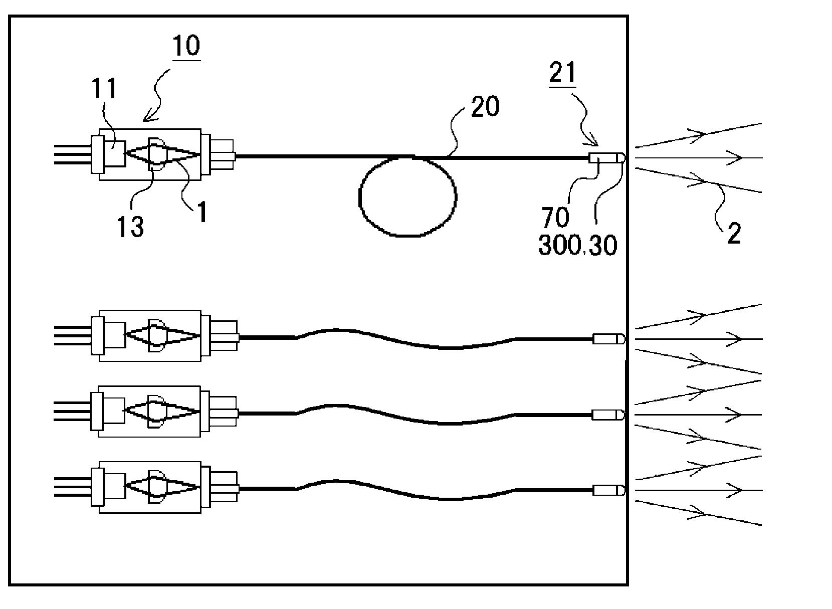
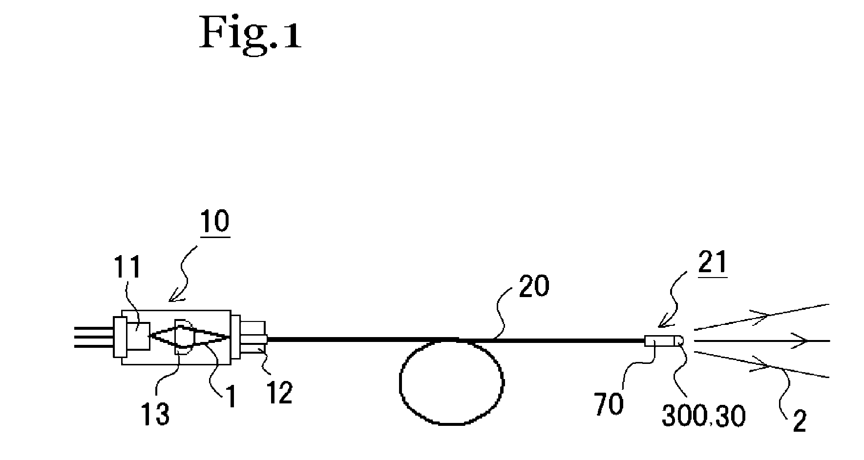
[0224] As shown in FIG. 1, the light emitting device of this embodiment is comprised of an excitation light source 10, a light guide 20, a thermally conductive transparent film (not shown in the figures), and a wavelength converting member 30.

[0225] The excitation light source 10 uses a laser diode as a light emitting element 11 which has an emission peak wavelength in the neighborhood of 405 nm. The laser diode is a GaN type semiconductor element.

[0226] The light guide 20 has one end which is connected to the light radiating part 12 of the excitation light source 10, and the other end is connected to an output part 21. The light guide 20 is made from quartz, for instance, Si 114 (μm: core diameter) / 125 (μm: clad diameter).

[0227] The end of the light guide 20 is equipped with an SUS ferrule.

[0228] Furthermore, an ITO film with a thickness of 3000 angstroms, which is the end surface of the ferrule, is placed on the whole surface of the light radiating surface of the light guide 3...

embodiment 2

[0239] The light emitting devices of this embodiment were essentially identical to the light emitting device of the first embodiment except that LAG, BAM, YAG, SCA, SCESN, SESN, CESN and CaAlSiN3:Eu were each used for the fluorescent material.

[0240] When these light emitting devices were similarly evaluated, nearly identical results were obtained for the relative intensity of light compared to the optic output and the device life.

embodiment 3

[0241] The light emitting device of this embodiment was identical to the light emitting device of the first embodiment except that the fluorescent material was made by mixing 10 g of Ca10(PO4)6Cl2:Eu, 100 g of isopropyl alcohol, 20 g of alumina sol, and 10 g of acetone, applying a voltage of 50 V, and then drying and using electrodeposition to apply the fluorescent material.

[0242] When these light emitting devices were similarly evaluated, nearly identical results were obtained for the relative intensity of light compared to the optic output and the device life.


PUM


Abstract

The present invention provides a light emitting device comprising: an excitation light source which radiates excitation light; a wavelength converting member which absorbs and converts the wavelength of at least part of the excitation light radiated from the excitation light source, and releases light with a predetermined wavelength band; a light guide for guiding the excitation light radiated from the excitation light source to the wavelength converting member, with one end at the excitation light source and the other end at the wavelength converting member, wherein the refractive index of the cross-sectional center region (core) is higher than that of the circumferential region (clad); and a thermally conductive transparent film which contacts with the wavelength converting member.

Description

BACKGROUND OF THE INVENTION [0001] 1. Field of the Invention [0002] The present invention relates to a light emitting device, and more particularly relates to light emitting device which has an excitation light source, a wavelength converting member, and a light guide. [0003] 2. Background Information [0004] Conventionally, endoscope devices, fiber scopes and the like require a light which represents a high luminance and accurate reproduction of color information. [0005] Therefore, the use of semiconductor light emitting elements such as light emitting diode elements (LED) and laser diode elements (LD) or the like have been proposed as light sources to replace xenon lamps or the like (for instance, JP 2002-95634-A and JP 2003-515899-A). [0006] Semiconductor light emitting elements are compact, have good power efficiency, and emit brilliant colored light. Furthermore, these elements are formed from semiconductors, so there is no concern about burning out. In particular, semiconductor...

Claims


Application Information

Patent Timeline
IPC IPC(8): H01S3/30H01S3/10H01S3/08
CPCA61B1/00096A61B1/0017A61B1/0653A61B1/07G02B6/262G02B6/4204G02B2207/113H01S5/02284A61B1/0669H01S5/2009H01S5/34333H01S5/4025H01S5/0087H01S5/02251
Inventor HAMA, ATSUTOMOTAKEICHI, JUNJISUGIYAMA, TAKAFUMIHAYASHI, YUKIHIRO
Owner NICHIA CORP
Why Eureka
Try Eureka