
Method for manufacturing semiconductor device

a manufacturing method and semiconductor technology, applied in the direction of semiconductor devices, basic electric elements, electrical appliances, etc., can solve the problem of isotropic etching of silicon nitride films, and achieve the effect of enhancing processing precision and suppressing the change of sidewalls in dimension

Inactive Publication Date: 2006-09-14
SEMICON ENERGY LAB CO LTD
View PDF24 Cites 62 Cited by
  • Summary
  • Abstract
  • Description
  • Claims
  • Application Information

AI Technical Summary

Benefits of technology

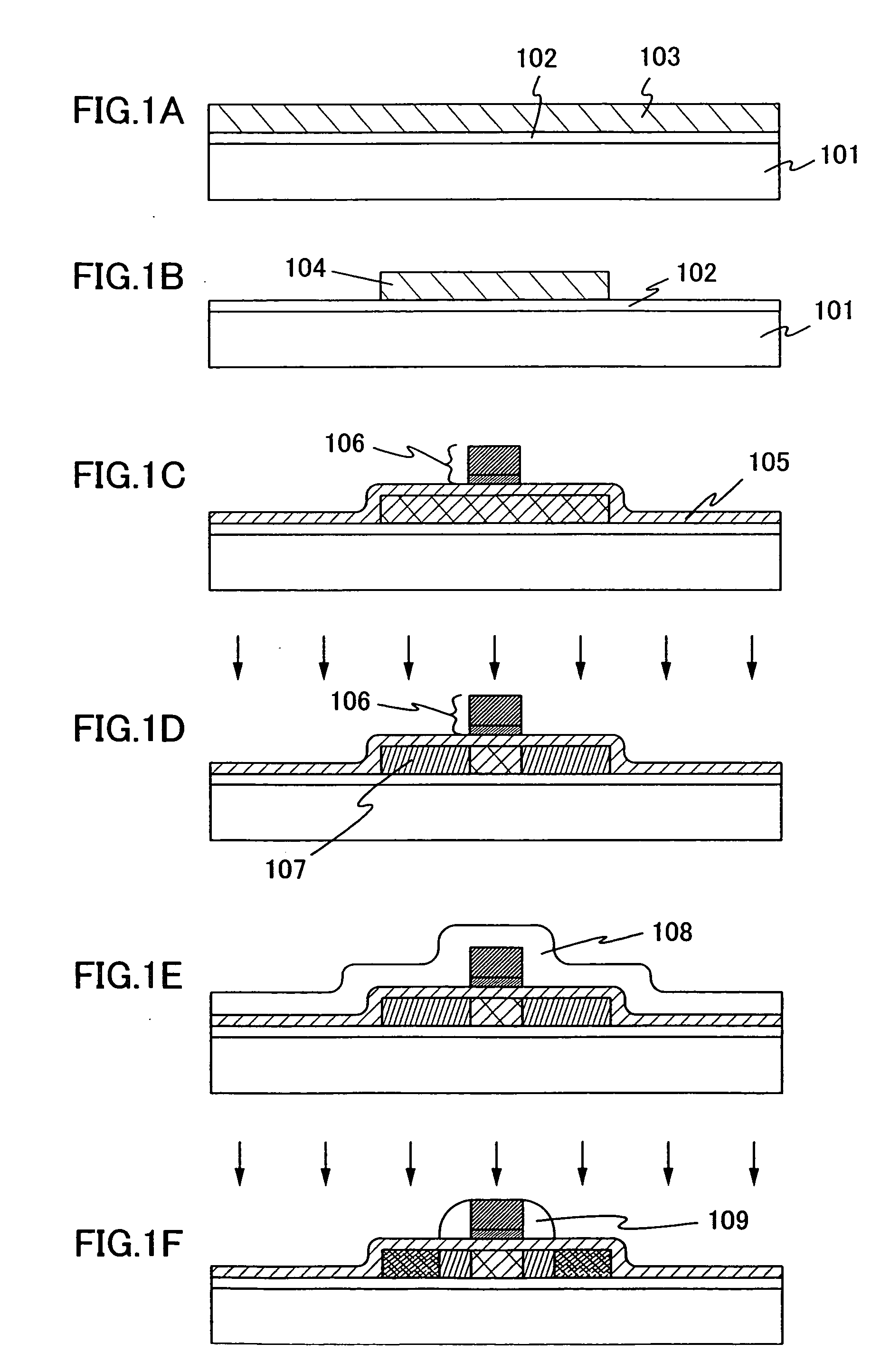
[0015] It is an object of the present invention to solve the above problem of the conventional technique. The object is to suppress change of a sidewall in dimension in etching a silicon nitride film and thus to enhance processing precision in forming an LDD region.
[0026] According to the present invention, higher anisotropy can be obtained in etching a silicon nitride film compared with the case where a gas containing a fluorine atom is used. Therefore, there can be less dimensional change in width of a sidewall when the silicon nitride film is etched. Further, it is possible to form an LDD region preferably in accordance with this sidewall.

Problems solved by technology

However, when etching of a silicon nitride film is performed with an RIE apparatus with the use of a gas containing a fluorine atom, the etching of a silicon nitride film is performed isotropically.

Method used


Image

  • Method for manufacturing semiconductor device
  • Method for manufacturing semiconductor device
  • Method for manufacturing semiconductor device

Examples


embodiment 1

[0068] A method for manufacturing a semiconductor element will be explained with reference to drawings. Note that the case of forming a semiconductor film in an insulating substrate and manufacturing a TFT with the use of this semiconductor film is shown in this embodiment.

[0069] As shown in FIG. 4A, a base film 402 is formed over a substrate 401 having an insulating surface. In this embodiment, a glass substrate is used as the substrate 401. Note that, as the substrate used here, a glass substrate such as a barium borosilicate glass or an alumino borosilicate glass, a quartz substrate, a ceramic substrate, a stainless steel substrate, or the like can be used. In addition, a substrate made from plastic typified by PET (polyethylene terephthalate), PES (polyethersulfone resin), or PEN (polyethylene naphthalate) or synthetic resin such as acryl as a raw material tends to have lower heat resistance than another substrate. Such a substrate can be used, as long as the substrate can resi...

embodiment 2

[0110] In this embodiment, a process of manufacturing a CMOS-type IC using a semiconductor substrate will be explained with reference to drawings.

[0111] Note that a semiconductor substrate used in this embodiment refers to a single-crystal silicon substrate or a compound semiconductor substrate, or an SOI (Silicon on Insulator) substrate. An N-type or P-type single-crystal silicon substrate, a GaAs substrate, an InP substrate, a GaN substrate, a SiC substrate, a sapphire substrate, a ZnSe substrate, or the like, can be typically given as the single-crystal silicon substrate or compound semiconductor substrate. A substrate manufactured by a pasting method, a SIMOX (Separation by Implanted Oxygen) method, or the like can be typically given as the SOI substrate. When a semiconductor element is manufactured using an SOI substrate, the adjacent elements can be separated completely; thus, the flowing of leak current can be prevented.

[0112] First, a substrate 800 made of single-crystal s...

embodiment 3

[0136] Here, a process of manufacturing a thin film integrated circuit or a non-contact thin film integrated circuit device (also referred to as a wireless IC tag or an RFID (Radio Frequency Identification)) is shown as an example of a semiconductor device manufactured according to the present invention, with reference to FIGS. 12A to 12D, FIGS. 13A to 13D, FIGS. 14A to 14C, FIGS. 15A to 15C, and FIGS. 16A and 16B.

[0137] Although an example of using electrically isolated TFTs as a semiconductor element used for an integrated circuit of a wireless IC tag is shown below, the semiconductor element used for the integrated circuit of the wireless IC tag is not limited to TFTs and any kinds of elements can be used. For example, besides TFTs, a storage element, a diode, a photoelectric conversion element, a resistor element, a coil, a capacitor element, an inductor, or the like is typically given.

[0138] First, a peeling layer 1201 is formed over a glass substrate (a first substrate) 1200...


PUM


Abstract

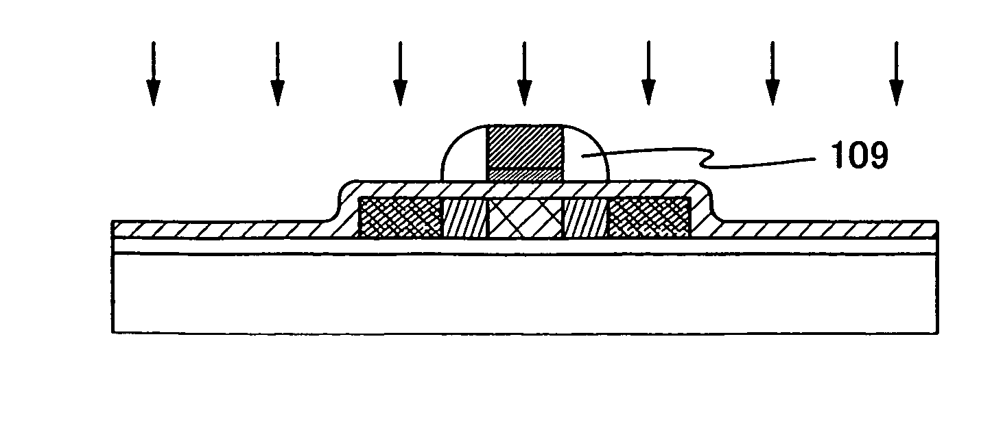
In a gas containing a fluorine atom in the molecule, etching of a SiN film is performed isotropically; therefore, the width of a sidewall gets smaller and it is difficult to widen the width of an LDD region. A silicon nitride film is formed over a gate electrode, a hydrogen bromide is mainly used as an etching gas, the silicon nitride film only over the gate electrode and the surface of a substrate are removed by an etching method such as ICP (Inductively Coupled Plasma), and the silicon nitride film is simultaneously left only on the side surface part of the gate electrode.

Description

BACKGROUND OF THE INVENTION [0001] 1. Field of the Invention [0002] The present invention relates to a method for forming a sidewall formed of silicon nitride on a side surface of a gate electrode, and to a semiconductor device manufactured through this process and a manufacturing method thereof in a manufacturing process of a thin film transistor (TFT). [0003] 2. Description of the Related Art [0004] Research and development have been widely conducted on size reduction and high integration of semiconductor elements. In particular, a technique for reducing the size of a MOS transistor has been remarkably advanced. MOS is an acronym of Metal-Oxide-Semiconductor, which shows a structure in which three kinds of materials (substances) of metal, oxide, and a semiconductor are combined. [0005] Here, the metal includes not only pure metal but also a semiconductor material having sufficiently high conductance, an alloy of a semiconductor and metal, or the like. The oxide includes not only p...

Claims


Application Information

Patent Timeline
IPC IPC(8): H01L21/8234
CPCH01L21/31116H01L21/823864H01L27/1214H01L27/1266H01L29/66757H01L29/78621H01L27/1277H01L27/127
Inventor SATO, TOMOHIKOMONOE, SHIGEHARU
Owner SEMICON ENERGY LAB CO LTD
Learn More