

Silicon wafer and process for the heat treatment of a silicon wafer
a technology of silicon wafers and heat treatment, which is applied in the direction of gel state, after-treatment details, and under a protective fluid, etc., can solve the problems of thermal stress, adverse effect on the function of the electronic components produced thereon, and ris
- Summary
- Abstract
- Description
- Claims
- Application Information
AI Technical Summary
Benefits of technology
Problems solved by technology
Method used
Image

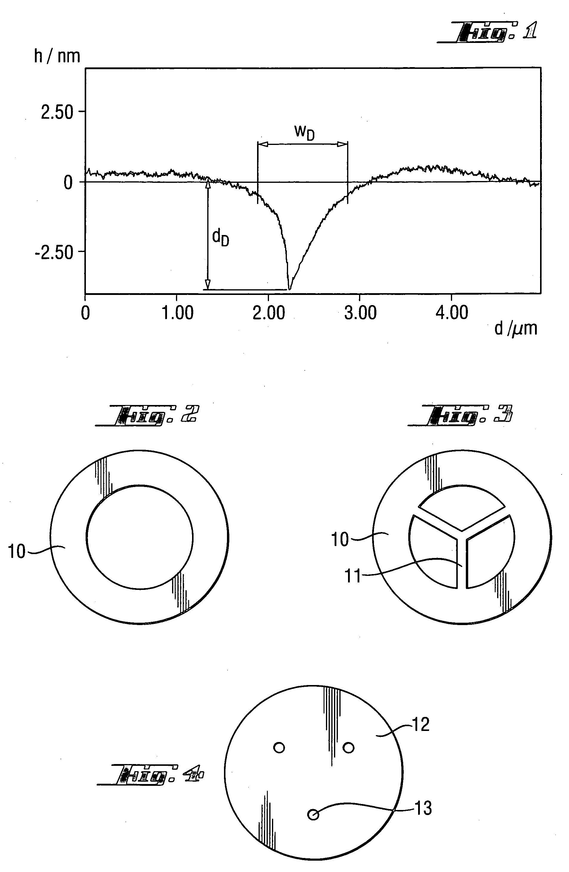
Examples
example 1
[0089] A single-crystal silicon ingot with a nitrogen concentration of 6·1013 atoms / cm3 at the start of the ingot and of 2.5·1014 atoms / cm3 at the end of the ingot, an interstitial oxygen concentration of from 6.5·1017 atoms / cm3 to 6.6·1017 atoms / cm3 and a resistivity of from 8 Ωcm to 12 Ωcm is pulled by the Czochralski process and cut into wafers. The wafers are polished. Based on the dopant concentrations, all the wafers can be classified as class 2 according to the invention. The silicon wafers are subjected to a heat treatment according to the invention in an atmosphere consisting of 100% argon with a holding time of 2 hours at 1200° C., during which heat treatment they rest on substrate holders with a roughness of Ra=0.15 μm, which are suitable for class 2. The heating and cooling rates are selected in such a way that at any temperature they correspond to the inequality given for class 2.
[0090] Then, a plurality of wafers which originated from different positions along the axi...
example 2
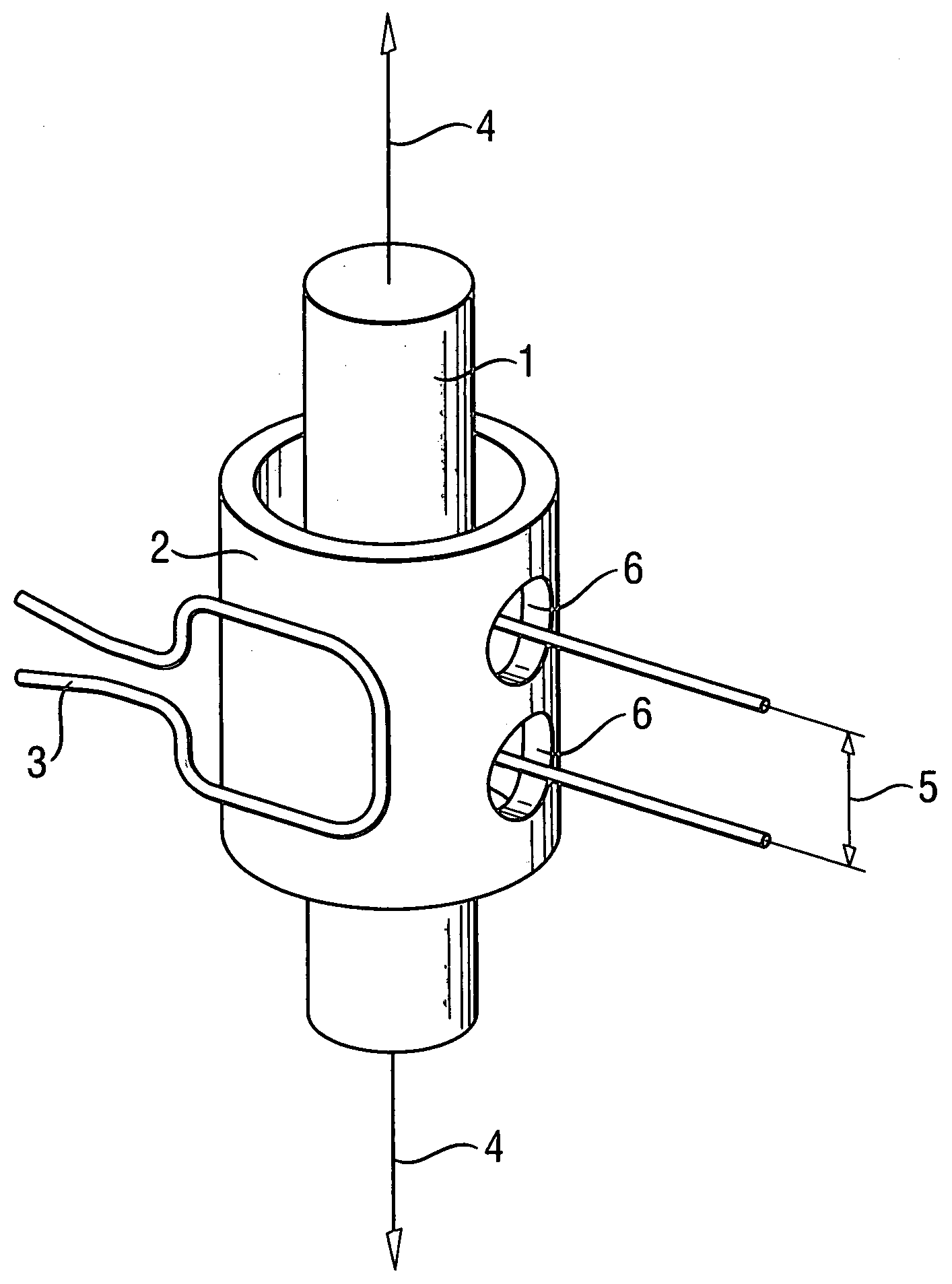
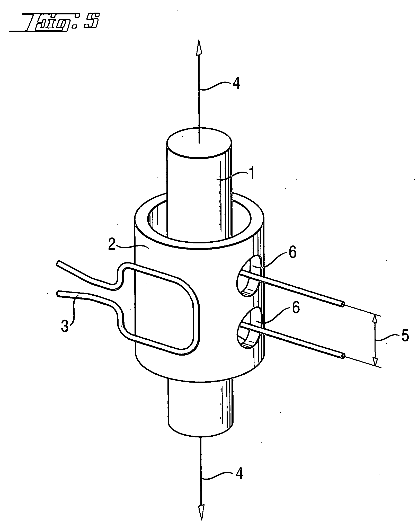
[0094] A single-crystal silicon ingot with a nitrogen concentration of 3·1013 atoms / cm3 at the start of the ingot and of 1.2·1014 atoms / cm3 at the end of the ingot, an interstitial oxygen concentration of on average 5.6·1017 atoms / cm3 and a resistivity of from 20 to 30 Ωcm is pulled using the Czochralski process and cut into wafers. The wafers are polished. The silicon wafers are subjected to a heat treatment according to the invention in an atmosphere consisting of 100% argon. The heat treatment comprises a heating operation, a treatment at a constant temperature of 1200° C. for two hours and a cooling operation, with ramp rates of from 1 to 10° C. / minute being adhered to during the heating and cooling operations. During the heat treatment, the silicon wafers are mounted on substrate holders made from silicon carbide, which are in the shape of a continuous concentric ring with or without an additional bearing surface in the center of the ring.
[0095] Then, a plurality of wafers whi...
PUM
| Property | Measurement | Unit |
|---|---|---|
| diameter | aaaaa | aaaaa |
| temperature | aaaaa | aaaaa |
| yield stress | aaaaa | aaaaa |
Abstract
Description
Claims
Application Information