Pore cathode for the mass production of photovoltaic devices having increased conversion efficiency

a photovoltaic device and mass production technology, applied in the direction of chemical vapor deposition coating, electric discharge tube, coating, etc., can solve the problems of high energy consumption, high temperature, time-consuming methods, and high cost of crystalline materials, and achieve high-quality photovoltaic semiconductor materials, increase the utilization of process gases, and enhance the effect of continuous deposition of photovoltaic modules

Inactive Publication Date: 2006-10-05
ENERGY CONVERSION DEVICES INC
View PDF3 Cites 8 Cited by
  • Summary
  • Abstract
  • Description
  • Claims
  • Application Information

AI Technical Summary

Benefits of technology

[0023] The present invention enhances continuous deposition of photovoltaic modules by providing a pore cathode for use in a plasma deposition chamber of a continuous roll-to-roll deposition system. The cathode of the invention distributes reaction gases in the plasma region bounded by the cathode and the active surface of a substrate. By providing a relatively large area (which may include a number of similar cathode modules used in conjunction with each other) and regular spacings of inlet pores and outlet pores for fresh and spent reaction gases, the device is able to deliver the gases uniformly across the entire active surface of a web-like substrate. The gas outlet pores of the inventive cathode are uniquely sized, shaped and spaced to provide new pla

Problems solved by technology

While solar cells, switches and the like having favorable characteristics continue to be so manufactured, it is recognized that preparation of crystalline materials introduces substantial costs into the semiconductor industry.
Single crystal silicon and the like must be produced by expensive, energy intensive, high-temperature, time-consuming methods.
In particular, solar cell technology, which is dependent upon the production of a large number of devices to comprise a panel, is critically affected by processing economies.
In addition to the aforementioned inherently “batch” nature of crystal growth, a substantial amount of the carefully grown material is lost in the sawing of the ingot into a plurality of useable wafers.
Substantial surface finishing and processing effort is often required thereafter.
As in the case of crystalline devices, such production methods impair the economic feasibility of amorphous devices such as solar cells by introducing “dead time” during which valuable equipment sits idle.
Unfortunately in the prior art, the rate of deposition of the precursor gas mixture remains constant.
Applicant has in the past seen that increasing the rate of deposition of semiconductor alloy material tends to decrease the photovoltaic properties of that material.
To prove this, one only needs to speed up (even slightly) the deposition of the amorphous silicon and note that one loses the photovoltaic efficiency very quickly.
The mistake of the prior art is that it does not change the chemical and electronic plasma conditions, which means that a different type of plasma is made by only changing the deposition throughput speed (without changing any of the properties/char

Method used


Image

  • Pore cathode for the mass production of photovoltaic devices having increased conversion efficiency
  • Pore cathode for the mass production of photovoltaic devices having increased conversion efficiency
  • Pore cathode for the mass production of photovoltaic devices having increased conversion efficiency

Examples


Embodiment Construction

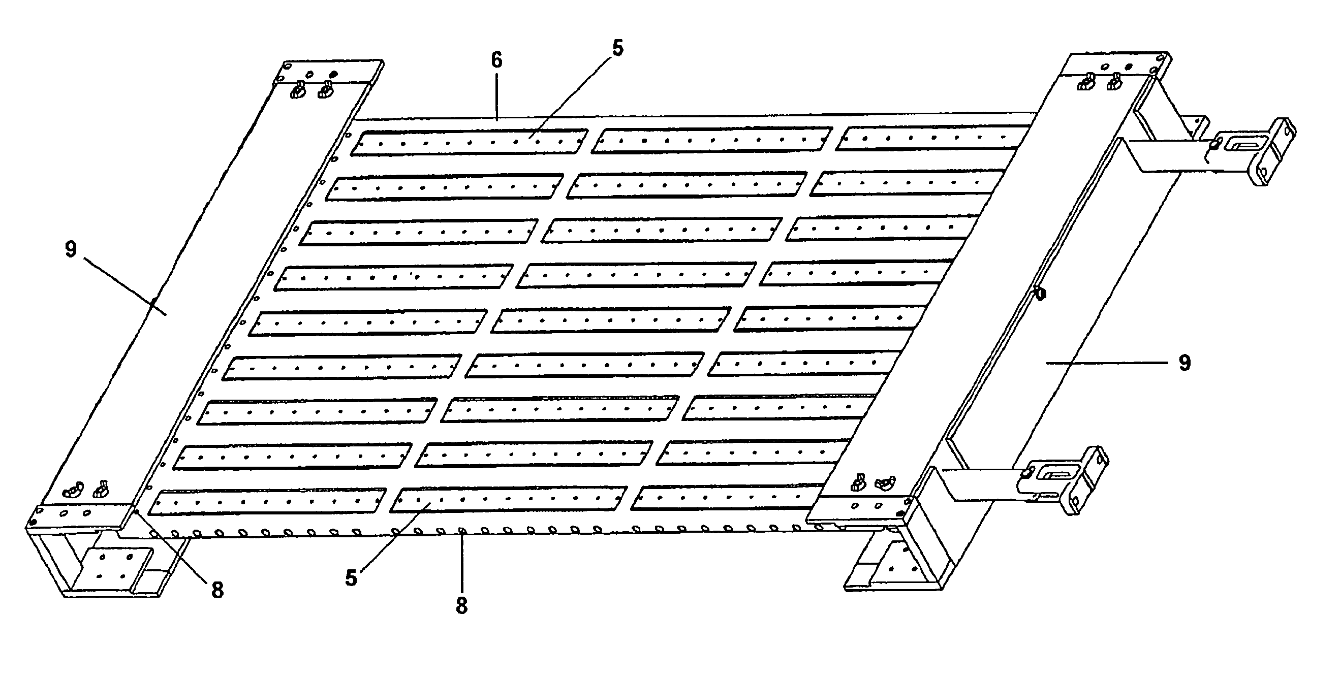
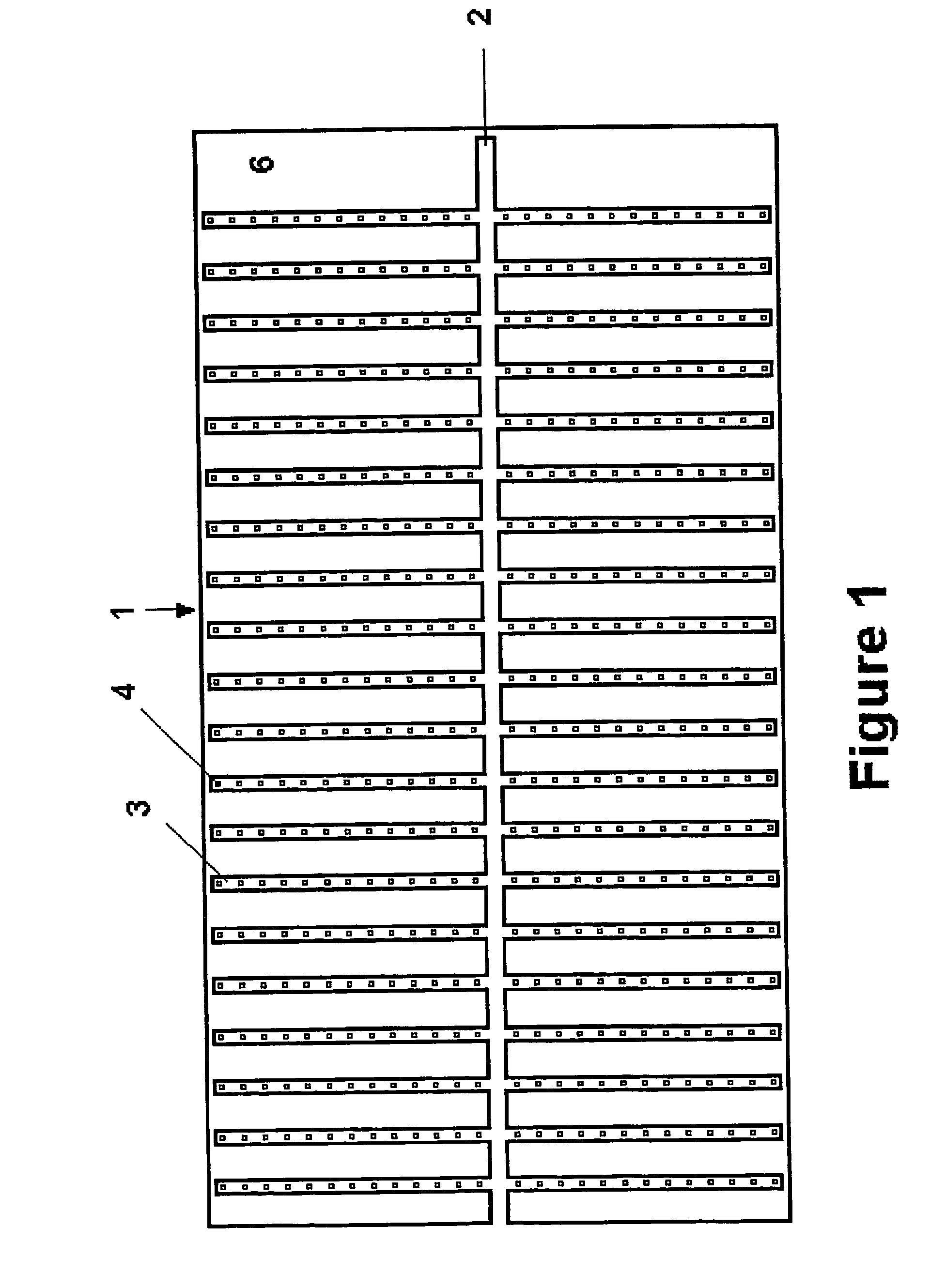
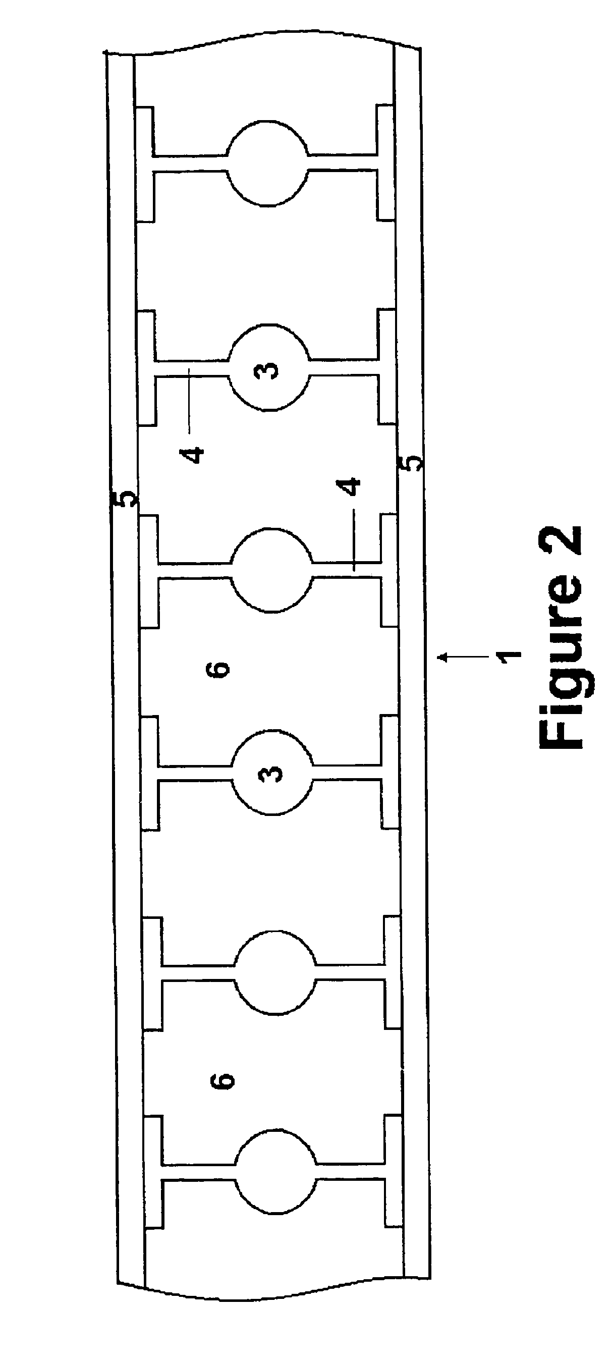
[0029] The present invention relates to a cathode for a deposition chamber for plasma enhanced deposition of large area, thin film semiconductor materials and deposition chambers incorporating such cathodes. Specifically the cathode is a planar pore cathode which serves the dual functions of (1) an electrode for the plasma deposition process and (2) a distribution conduit for the flow of fresh reaction gas to and for the evacuation of the spent reaction gas from the plasma region to maintain a uniform, constant pressure plasma reaction. The cathode is electrically connected to the RF power source. The cathode is preferably vertically mounted and contains gas dispersion plates to prevents direct, line-of-sight, flow of process gases to the adjacent deposition substrate (which acts as the anode in the deposition) and more uniformly distributes the gases flowing into the plasma region between the cathode and the substrate. By providing a relatively large area (which may include a numbe...


PUM

PropertyMeasurementUnit
Lengthaaaaaaaaaa
Lengthaaaaaaaaaa
Efficiencyaaaaaaaaaa

Abstract

A pore cathode for use in a deposition chamber for the plasma enhanced deposition of photovoltaic materials onto one or more webs of substrate material. The cathode is planar and serves the dual functions of (1) an electrode for the plasma deposition process and (2) a distribution conduit for the flow of fresh reaction gas to and for the evacuation of the spent reaction gas from the plasma region to maintain a uniform, constant pressure plasma reaction. The gas outlet pores of the inventive cathode are uniquely sized, shaped and spaced to provide new plasma chemistry and physics to insure optimization of the zoo of chemical species within the plasma regardless of deposition speed. That is, the distribution of ions, electrons, free radicals and neutral species in the plasma are optimized to deposit high quality photovoltaic semiconductor material while also increasing the utilization of the process gases, thus allowing the economical mass production of amorphous silicon solar cells having at least 8% photovoltaic efficiency on large area substrates. The pores can be covered by gas dispersion plates which prevent direct, line-of-sight, flow of the process gases to the adjacent deposition substrate and more uniformly distributes the gases flowing into the plasma region between the cathode and the substrate, thus minimizing the effects of non-homogeneity of the depositing species.

Description

RELATED APPLICATIONS [0001] The present application is a continuation-in-part of U.S. patent application Ser. No. 10 / 043,010 filed Jan. 11, 2002, the disclosure of which is incorporated herein by reference.FIELD OF THE INVENTION [0002] The present invention relates to apparatus and systems which may be utilized to mass-produce thin film semiconductor devices and more specifically to a unique pore cathode which allows for fundamentally new plasma physics and chemistry along with greater uniformity of deposited semiconductor materials in plasma assisted deposition. The size and distribution of the gas outlet pores allows for uniquely synergistic plasma constituent ratios (i.e. the ratio of ions, neutrals and free radicals as well as the composition of the ions, neutrals and free radicals) and sets the boundary conditions for the plasma, resulting in a controlled plasma by utilizing small pore gas outlets from which the plasma is formed. This, in turn, allows for the deposition of phot...

Claims


Application Information

Patent Timeline
IPC IPC(8): C23C16/00C23C16/44C23C16/455C23C16/509H01J37/32
CPCC23C16/4412C23C16/45565H01J37/32541H01J37/3244C23C16/5096
Inventor OVSHINSKY, STANFORD R.
Owner ENERGY CONVERSION DEVICES INC
Why Eureka
Try Eureka