Boost converter utilizing bi-directional magnetic energy transfer of coupling inductor

a technology of coupling inductor and magnetic energy transfer, which is applied in the direction of dc-dc conversion, power conversion systems, instruments, etc., can solve the problems of high switch loss, inability to solve easily, and inability so as to reduce the power consumption of the diode, reduce the cost of the diode, and increase the load

Active Publication Date: 2006-10-12
YUAN ZE UNIV
View PDF3 Cites 81 Cited by
  • Summary
  • Abstract
  • Description
  • Claims
  • Application Information

AI Technical Summary

Benefits of technology

[0020] 8. The capacity of coupling inductor is smaller than traditionally used circuit. Coupling inductor has the same character as transformer, where once current pass primary winding there will be output current in secondary winding. According to analysis of idealized transformer, energy transferred to secondary winding makes magnetic flux equals to zero in iron core and does not increase any load on iron core's magnetic flux. The magnetic excited current in primary winding will pass onto secondary winding when semi-conductor power switch is turned off according to flyback transformer theory; the current in the secondary winding then charges filter circuit in reverse at a much lower current. Normally to produce low ripple charging current, transformer must have high induction value, while low induction design by the present invention means substantially decreasing current ripples in semi-conductor power switch and reducing required iron core's capacity.
[0021] 9. Relative low transformer copper loss. The configuration of the present invention allows high ripples in magnetic excited current and low magnetic excited coupling induction, which requires less turns of primary winding where large current pass through, reducing copper loss generated by surface skin effects and magnetic excited loss.
[0022] 10. Easy to handle magnetic interference. Rapidly changing current is limited to primary circuit, making it easy to handle magnetic interference.

Problems solved by technology

Increasing the turn ratio of winding can obtain relative low switch clamping voltage and lenient duty cycle control while endurance of the diode at high voltage side can not be solved easily, specially, when switching spike voltage from high voltage side winding; furthermore, if duty cycle is too low induction current will be in non-continuous form and increases of ripples making current into see-saw waveforms, for example, since MOSFET switch conduction loss is proportional to the square of the current, under the same supplied power, see-saw current waveforms make higher switch loss than square waveforms.
First, since only a few moments to transfer all the energy, the diode has to endure large transient current; second, because above mentioned spike voltage problem, the switching duty cycle is too high, and the diode's capacity has to be increased such that the loss increases too.
In a nutshell, increasing the turn ratio of winding to gain high boost rate is not ideal.
The energy in the capacitor of the passive snubber is consumed completely by the resistor, therefore it has lowest efficiency.
Because power equals to voltage multiplying current, when current is very high at a low voltage DC power source, spike voltage can be induced by a little distributed inductance, which comes from improper wire layout, inner induction of wire and components.
Having a high current and low induction wiring layout can be a challenge in practice, and present circuit effectively reduces induction between wires.

Method used


Image

  • Boost converter utilizing bi-directional magnetic energy transfer of coupling inductor
  • Boost converter utilizing bi-directional magnetic energy transfer of coupling inductor
  • Boost converter utilizing bi-directional magnetic energy transfer of coupling inductor

Examples


Embodiment Construction

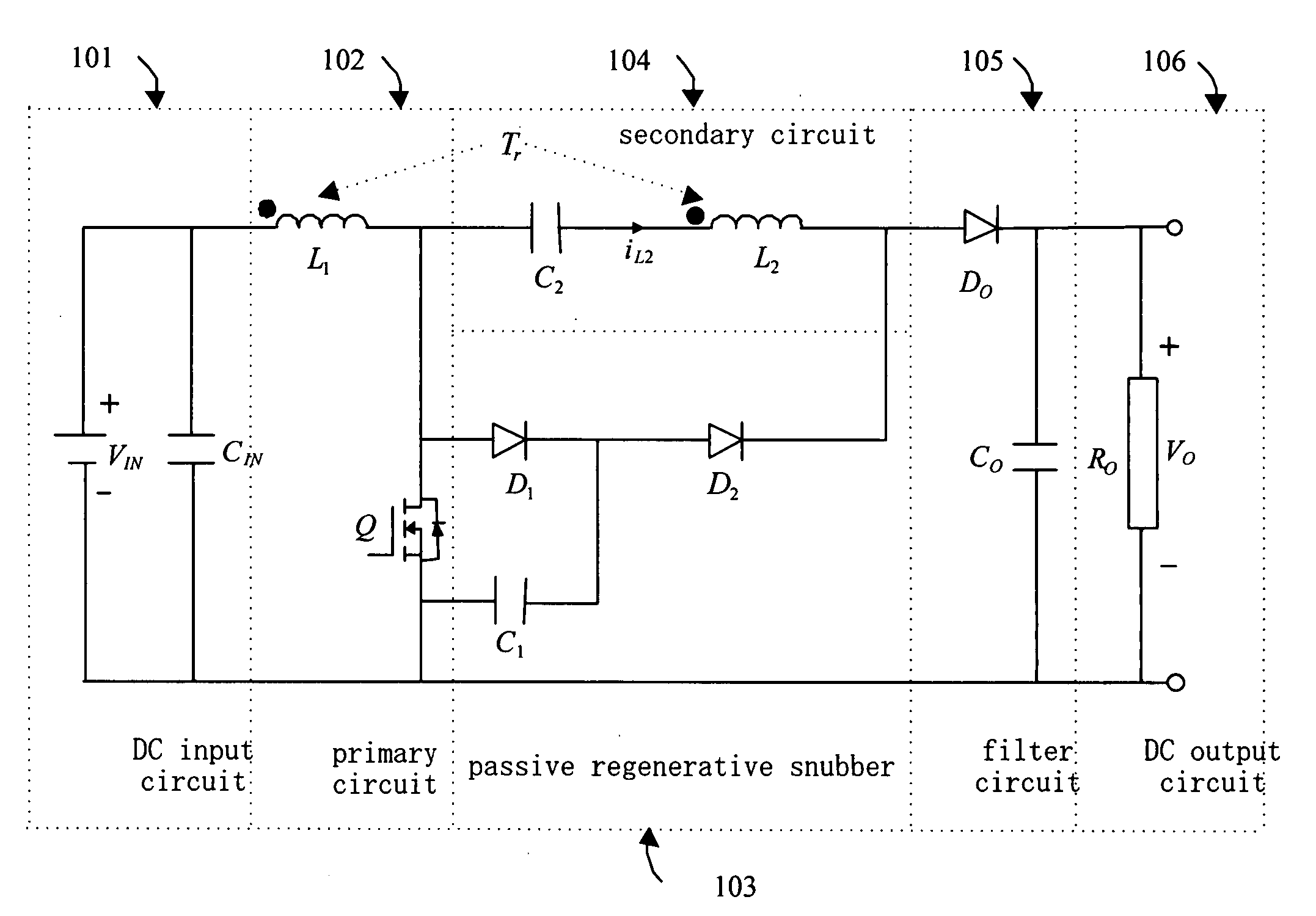
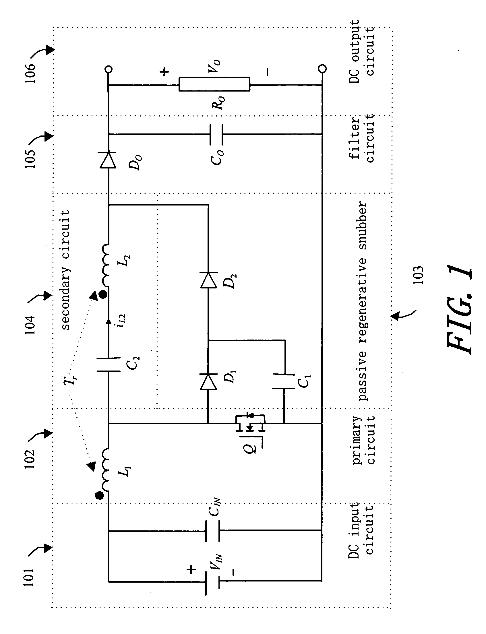
[0048] The first preferred embodiment of the present invention is shown in FIG. 1. DC voltage VIN of DC input current circuit 101 stores energy in primary winding L1 of coupling inductor Tr when semi-conductor power switch Q of primary circuit 102 is turned on; at the same time, because bi-directional current path of secondary winding L2 of the coupling inductor Tr of secondary circuit 104, its induction voltage vL2 (polar point is positive at the moment) plus the voltage of clamping capacitor C1 of passive regenerative snubber 103 charge the high voltage capacitor C2 (charging current is −iL2) of secondary circuit 104 through semi-conductor power switch Q and discharge diode D2 route. At the instant when semi-conductor power switch Q is turned off, the current from primary circuit 102 leaves semi-conductor power switch Q, through the clamping diode D1 of passive regenerative snubber 103, into its clamping capacitor C1. According to the theorem that magnetic flux does not extinguish...


PUM


Abstract

A boost converter utilizing bi-directional magnetic energy transfer of coupling inductor provides a high efficiency boost DC-DC converting with above 30 times voltage boost rate, which uses a coupling inductor and low voltage switch to absorb circuit induction voltage of a passive regenerative snubber no matter if switch is turned on or off. Such that, a much higher voltage boost rate than the turn rate of transformer and wider range of switching duty cycle is obtained. A bi-directional magnetic energy path is utilized, that is, when switch is turned on the first winding of coupling inductor stores magnetic excited high current energy, and opposite magnetic flux is induced on the second winding at the same time. When switch is turned off the magnetic excited current continues and increases the voltage on the second winding. The second winding has bi-directional magnetic current induced and fully utilizes capacity of transformer's iron core.

Description

BACKGROUND OF THE INVENTION [0001] In many power supply applications, such as gas discharging light bulb, high-voltage DC bus of inverter in un-interrupt power supply and wide-frequency traveling wave tube amplifier etc, high-voltage DC power supplies are needed where rechargeable batteries provide power source; also, clean energy sources, such as solar power, wind power and fuel-cell battery, have relative low output voltages of DC power sources. It is necessary to have high-efficiency high voltage boost ratio DC-DC converter as front-end conversion mechanism. The present invention comprises a high voltage boost ratio converter, which utilizes bi-directional coupling induction magnetic energy transfer, such that: (1) converting traditional rechargeable battery and clean energy supply system into high-voltage DC power supply systems and substantially increasing energy efficiency and stability of power source; (2) after converting AC to DC boosting the voltage to thousand volt, or ad...

Claims


Application Information

Patent Timeline
Patent Type & Authority Applications(United States)
IPC IPC(8): G05F1/00
CPCH02M1/34H02M3/158H02M2003/1552H02M3/1552
Inventor WAI, RONG-JONGDUAN, ROU-YONG
Owner YUAN ZE UNIV
Why Eureka
Try Eureka