Semiconductor Lasers in Optical Phase-Locked Loops

a semiconductor laser and phase-locked loop technology, applied in semiconductor lasers, laser details, electrical equipment, etc., can solve the problems of lasers with potential for frequency mode-hopping, phase inversion and hysteresis, and many important electronic components, so as to increase optical power, high optical power, and high electrical efficiency

Inactive Publication Date: 2006-10-26
TELARIS
View PDF6 Cites 141 Cited by
  • Summary
  • Abstract
  • Description
  • Claims
  • Application Information

AI Technical Summary

Benefits of technology

[0032] In this invention, we disclose phase-locked semiconductor lasers whose optical phase and frequency characteristics are precisely controlled by use of high speed integrated circuits. Potential single frequency semiconductor laser elements include the vertically cavity surface emitting laser (VCSEL) and distributed feedback laser (DFB). For example, an emitter may be comprised of a two section DFB oscillator driven in an asymmetric, push-pull configuration to provide controlled and well-behaved frequency modulation response. The lasers are arranged as individual elements, bars, or two dimensional arrays. In a further example, each DFB laser includes a tapered, electrically pumped optical amplifier section to increase the optical power.
[0033] Laser designs which satisfy the unique requirements of phase-locking advantageously provide for high optical power, high ele...

Problems solved by technology

However, several important electronic components, namely the voltage controlled oscillator (VCO) or current controlled oscillator (CCO), do not have high performance optical equivalents.
However, the frequency of semiconductor lasers depends in a relatively complex way on the level of injection current and these lasers exhibit the potential for frequency mode-hopping, phase inversion and hysteresis.
The competition between thermal tuning and electronic plasma tuning is known to be a significant ba...

Method used


Image

  • Semiconductor Lasers in Optical Phase-Locked Loops
  • Semiconductor Lasers in Optical Phase-Locked Loops
  • Semiconductor Lasers in Optical Phase-Locked Loops

Examples


Embodiment Construction

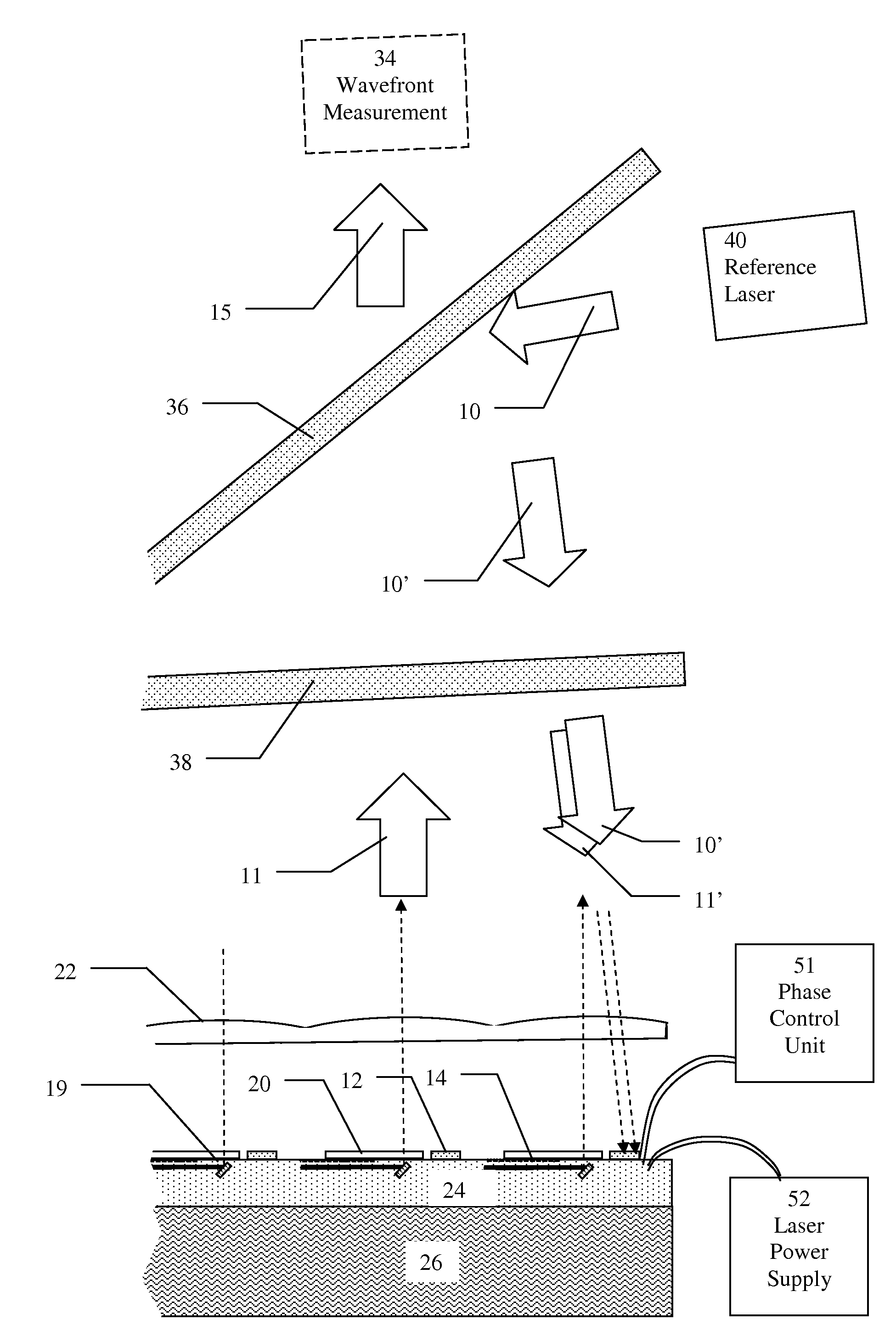
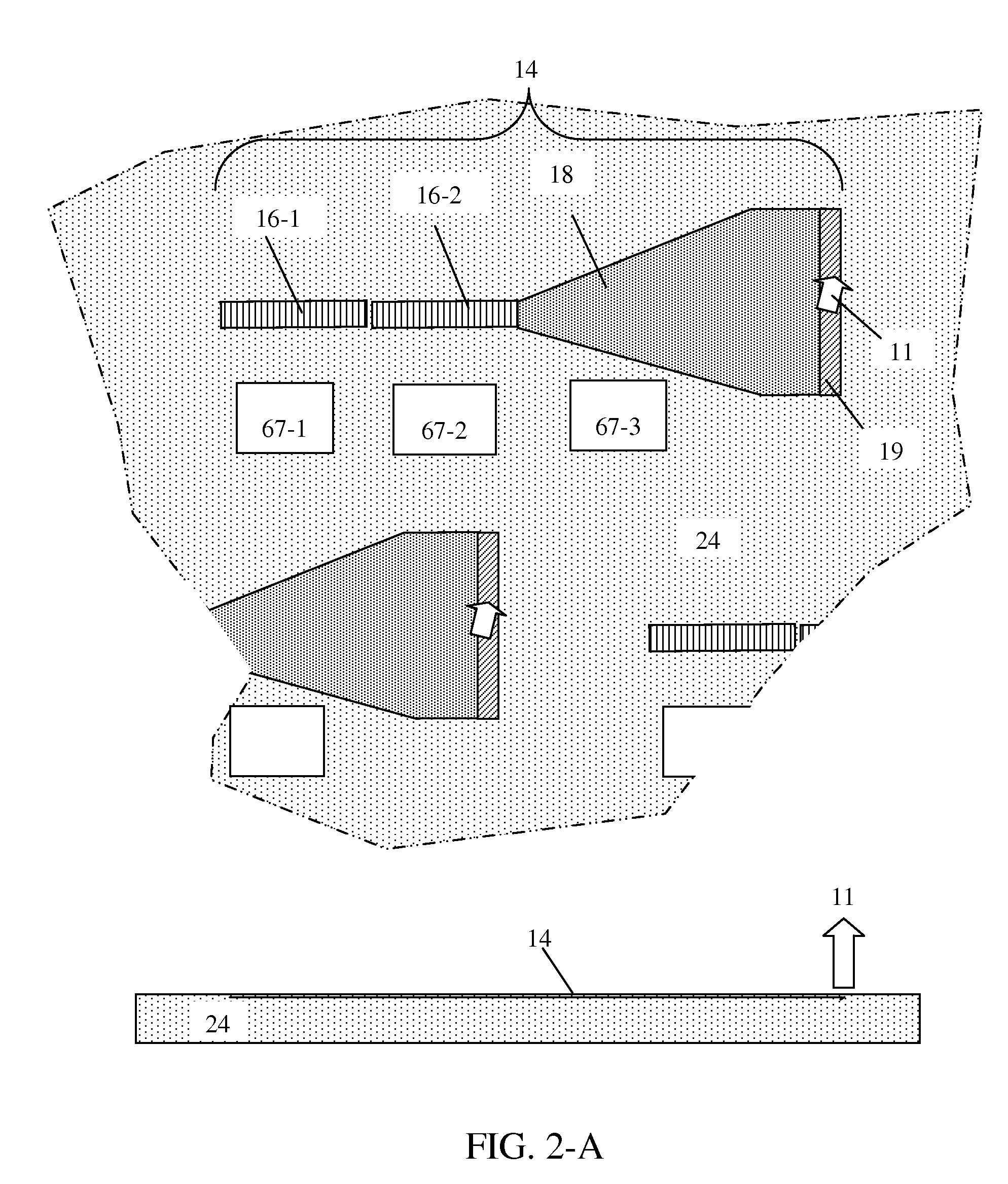
[0034] In this invention we disclose techniques for coherent optical beam combining of one or two dimensional semiconductor laser arrays driven by optical phase-locked loops (OPLLs). FIG. 1 illustrates a laser system comprised of a two dimensional array of vertically emitting, single-mode DFB lasers 24. Coherent combining of the laser output beams 1-j, where j denotes a particular emitter, is accomplished by integrating high-speed CMOS or SiGe BiCMOS circuitry 20 with integrated optical detectors 12 to electronically drive the ensemble of laser emitters 14 under conditions of phase and frequency lock. The laser array 24 is powered by an external electrical current supply 52 and backside cooled by use of element 26 in intimate thermal contact. The individual optical output beams 11-j are directed out of the plane of array 24 by individual etched steering mirrors 19. The use of etched mirrors for directing a laser's output normal to the substrate plane has been described by Osowski et...


PUM


Abstract

This invention relates to opto-electronic systems using semiconductor lasers driven by feedback control circuits that control the laser's optical phase and frequency. Feedback control provides a means for coherent phased laser array operation and reduced phase noise. Systems and methods to coherently combine a multiplicity of lasers driven to provide high power coherent outputs with tailored spectral and wavefront characteristics are disclosed. Systems of improving the phase noise characteristics of one or more semiconductor lasers are further disclosed.

Description

REFERENCE TO RELATED APPLICATIONS [0001] This application relies for priority on provisional application 60 / 674,093 of Yariv et al., filed on Mar. 23, 2005 and entitled “Optical phase-locked loops,” on provisional application 60 / 692,853 of Kewitsch et al., filed on Jun. 22, 2005 and entitled “Mode-locked semiconductor laser array,” and on provisional application 60 / 776,773 of Kewitsch et al., filed on Feb. 24, 2006 and entitled “Arrayed semiconductor lasers in optical phase-locked loops.”FIELD OF THE INVENTION [0002] This invention relates to opto-electronic systems using semiconductor lasers driven by feedback control circuits which control the laser's optical phase and frequency. Feedback control provides a means for coherent phased array operation and reduced phase noise. BACKGROUND OF THE INVENTION [0003] The optical analogs of electronic components such as amplifiers and filters have undergone significant advances with the development of wavelength division multiplexed optical ...

Claims


Application Information

Patent Timeline
IPC IPC(8): H01S3/13H01S3/00H01S5/00
CPCH01S3/0064H01S2301/206H01S3/1304H01S5/005H01S5/0264H01S5/042H01S5/0656H01S5/06821H01S5/0683H01S5/4062H01S5/4081H01S5/42H01S5/423H01S5/50H01S3/10053
Inventor KEWITSCH, ANTHONYRAKULJIC, GEORGEYARIV, AMNON
Owner TELARIS
Why Eureka
Try Eureka