Organic transistor, manufacturing method of semiconductor device and organic transistor

a manufacturing method and organic technology, applied in semiconductor/solid-state device manufacturing, basic electric elements, electric devices, etc., can solve problems such as high tunnel leakage current, difficult to use plastic or film as a substrate, and concern about reliability degradation, so as to reduce the tunnel leakage current, reduce the cost, and improve the effect of quality

Inactive Publication Date: 2006-11-30
SEMICON ENERGY LAB CO LTD
View PDF58 Cites 59 Cited by
  • Summary
  • Abstract
  • Description
  • Claims
  • Application Information

AI Technical Summary

Benefits of technology

[0010] It is an object of the present invention to provide a lower tunnel leakage current organic transistor by forming a dence and highly insulating resistance property gate insulating film than the gate insulating film formed by using a conventional CVD method.
[0024] Since a gate insulating film which is formed by using dense plasma can be a high quality film which is less damaged by plasma and has almost no defects, the gate insulating film can reduce a tunnel leakage current. Therefore, a highly reliable organic transistor can be obtained. In addition, when the conductive layer which becomes a gate electrode is insulated to be the gate insulating film, high integration is enabled.

Problems solved by technology

Since a high-temperature treatment is needed for forming a film of an inorganic semiconductor material as a semiconductor layer, it is difficult to use plastic or a film as a substrate.
However, when the gate insulating film is made thinner, a tunnel leakage current is high, and there is a concern about degradation of reliability.

Method used


Image

  • Organic transistor, manufacturing method of semiconductor device and organic transistor
  • Organic transistor, manufacturing method of semiconductor device and organic transistor
  • Organic transistor, manufacturing method of semiconductor device and organic transistor

Examples


embodiment mode 1

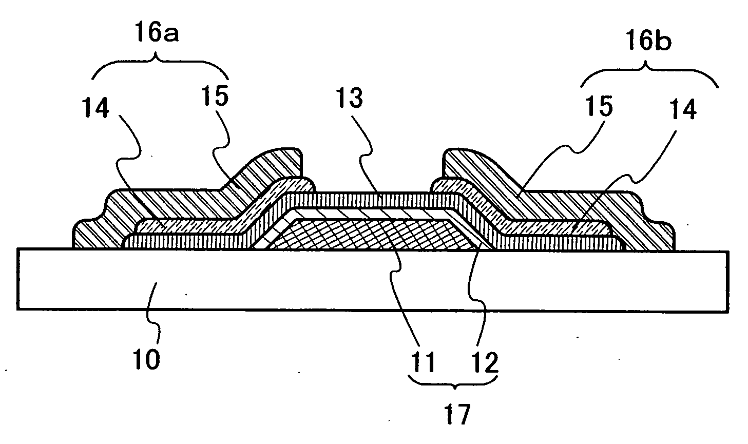
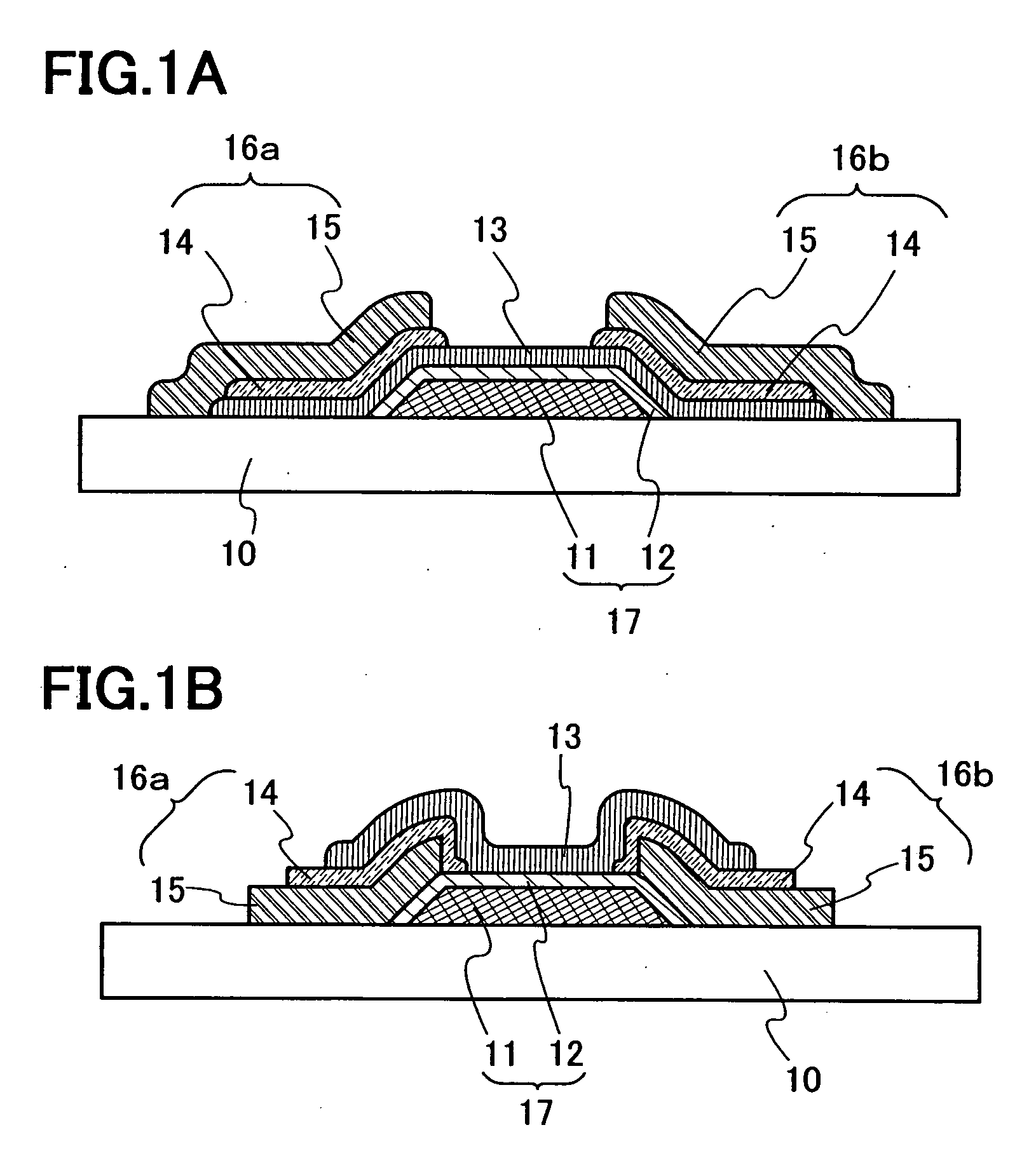
[0036] A configuration of an organic transistor structure of the present invention is shown in FIGS. 1A and 1B. Note that reference numeral 10 is a substrate, 11 is a gate electrode, 12 is a gate insulating film, 13 is a semiconductor layer including an organic semiconductor material, 14 is a composite layer having an organic compound and a metal oxide, 15 is a conductive layer, and a source and a drain electrodes 16a and 16b have a composite layer 14 and a conductive layer 15. Arrangement of each layer and electrode can be selected suitably depending of the use of the element. In addition, the composite layer 14 is formed to be in contact with the semiconductor layer 13 in FIGS. 1A and 1B; however, without being limited to this, the composite layer may be included in a portion of a source electrode and / or a drain electrode.

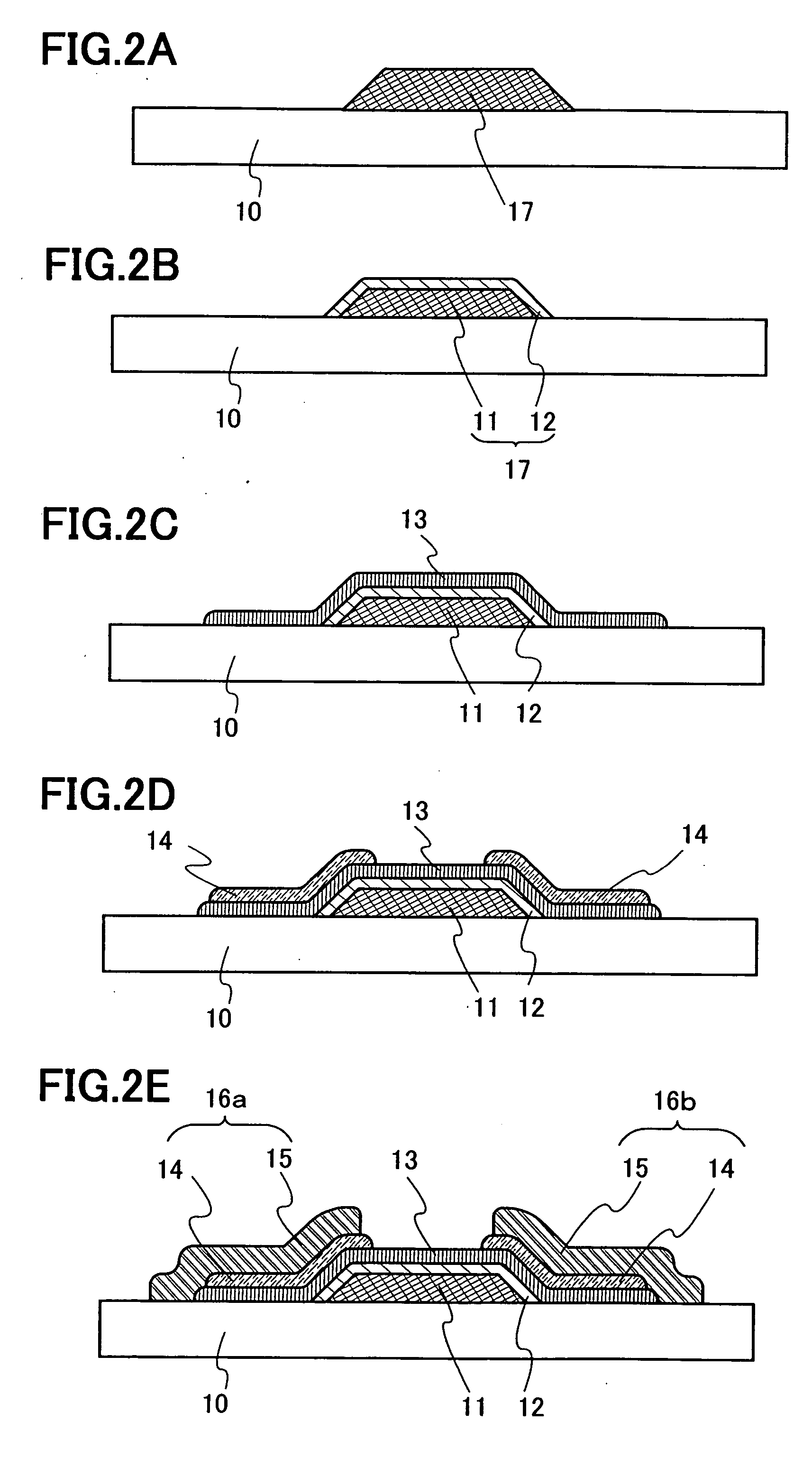
[0037] A structure of FIG. 1A is explained along manufacturing methods of FIGS. 2A to 2E. As the substrate 10, an insulating property substrate such as a glass ...

embodiment mode 2

[0061] The organic transistor as shown in embodiment mode 1 uses the insulating film formed by performing dense plasma treatment to the conductive layer which becomes the gate electrode as the gate insulating film; however, in this embodiment mode, a gate insulating film is formed by nitriding or oxygenizing with dense plasma additionally to the insulating film formed previously like FIGS. 3A and 3B. Since, elements except the gate insulating film and the gate electrode are similar to those of Embodiment Mode 1, they are denoted by the same reference numerals and the description thereof is omitted.

[0062] A gate electrode 31 is formed over a substrate 10. A material using for the gate electrode 31 is not limited particularly. For example, a metal such as gold, platinum, aluminum, tungsten, titanium, copper, molybdenum, tantalum, niobium, chromium, nickel, cobalt, magnesium and an alloy including them, a conductive high molecular compound such as polyaniline, polypyrrole, polythiophe...

embodiment mode 3

[0074] In this embodiment mode, an organic transistor having a structure which is different from the structure denoted in Embodiment Modes 1 and 2 is explained using FIGS. 4A and 4B. The organic transistor of the embodiment modes 1 and 2 is the bottom gate type transistor; however, the transistor of this embodiment mode is a top gate type transistor. Portions similar to those of Embodiment Mode 1 are denoted by the common reference numerals and the description thereof is omitted.

[0075] A structure of FIG. 4A is explained. The semiconductor layer 13 is formed over the substrate 10. Further, the source and drain electrodes 16a and 16b having the composite layer 14 and the conductive layer 15 are formed over the semiconductor layer 13.

[0076] Next, an insulating film 42 covering the semiconductor layer 13 and the source and drain electrodes 16a and 16b is formed. An inorganic material such as silicon oxide, silicon nitride or silicon oxynitride is used for the insulating film 42. Thes...


PUM


Abstract

It is an object to form a high quality gate insulating film which is dense and has a strong insulation resistance property, and to propose a high reliable organic transistor in which a tunnel leakage current is little. One mode of the organic transistor of the present invention has a step of forming the gate insulating film by forming the conductive layer which becomes the gate electrode activating oxygen (or gas including oxygen) or nitrogen (or gas including nitrogen) or the like using dense plasma in which density of electron is 1011 cm−3 or more, and electron temperature is a range of 0.2 eV to 2.0 eV with plasma activation, and reacting directly with a portion of the conductive layer which becomes the gate electrode to be insulated.

Description

BACKGROUND OF THE INVENTION [0001] 1. Field of the Invention [0002] The present invention relates to an organic transistor and a manufacturing method of an organic transistor having an organic semiconductor layer and a semiconductor device having an organic transistor. [0003] 2. Description of the Related Art [0004] A field-effect transistor controls an electric conductivity of a semiconductor layer which is provided between a source and a drain electrodes with a voltage applied to a gate electrode, and a field-effect transistor is a representative one of unipolar elements using carrier transport of either holes or electrons. [0005] Since various kinds of switching elements and amplifying elements can be formed depending on a combination of such field-effect transistors, these field-effect transistors are applied in various fields. For example, a switching element of a pixel in an active matrix display or the like can be given as the application. [0006] An inorganic semiconductor ma...

Claims


Application Information

Patent Timeline
Patent Type & Authority Applications(United States)
IPC IPC(8): H01L21/00
CPCH01L21/31683H01L51/0055H01L51/0525H01L51/0512H01L51/0545H01L51/0566H01L51/0002H01L51/0541H01L21/02244H01L21/02252H01L21/02247H01L21/02175H10K85/623H10K10/472H10K10/488H10K10/464H10K10/466H10K10/462H10K71/10
Inventor IMAHAYASHI, RYOTAFURUKAWA, SHINOBUISOBE, ATSUOARAI, YASUYUKIYAMAZAKI, SHUNPEI
Owner SEMICON ENERGY LAB CO LTD
Why Eureka
Try Eureka