Method for fabricating semiconductor device

Inactive Publication Date: 2006-12-28
SK HYNIX INC
View PDF9 Cites 3 Cited by
  • Summary
  • Abstract
  • Description
  • Claims
  • Application Information

AI Technical Summary

Benefits of technology

[0016] It is, therefore, an object of the present invention to provide a method for fabricating a semiconductor device capable of making a bit line pattern aligned with contact plug for a metal line by increasing a line width of the bit line pattern.
[0017] In accordance with one aspect of the present invention, there is provided a method for fabricating a semiconductor device, including: sequentially forming etch target layers, a hard mask layer and an anti-reflective coating layer; selectively etching the anti-reflective coating layer and the hard mask layer using a gas generating polymers, thereby increasing a line width of a bottom portion of the hard mask layer due to the polymers; and etching the etch target layers using a patterned hard mask layer with the increased line width.

Problems solved by technology

Due to the decreased channel length, a design margin for an internal pressure is reduced and thus, a plug concentration cannot get higher.
Furthermore, a driving current is also reduced due to the above described reasons and accordingly, a device degradation phenomenon such as a tWR fail of a semiconductor device and degradation in a refresh property are generated.
Furthermore, if the bit line pattern is formed through the conventional method, it may be difficult to obtain an effective line width of the bit line pattern.
Accordingly, a region adjacent to the bit line pattern may be damaged.

Method used


Image

  • Method for fabricating semiconductor device
  • Method for fabricating semiconductor device
  • Method for fabricating semiconductor device

Examples


Embodiment Construction

[0021] Hereinafter, detailed descriptions on certain embodiments of the present invention will be provided with reference to the accompanying drawings.

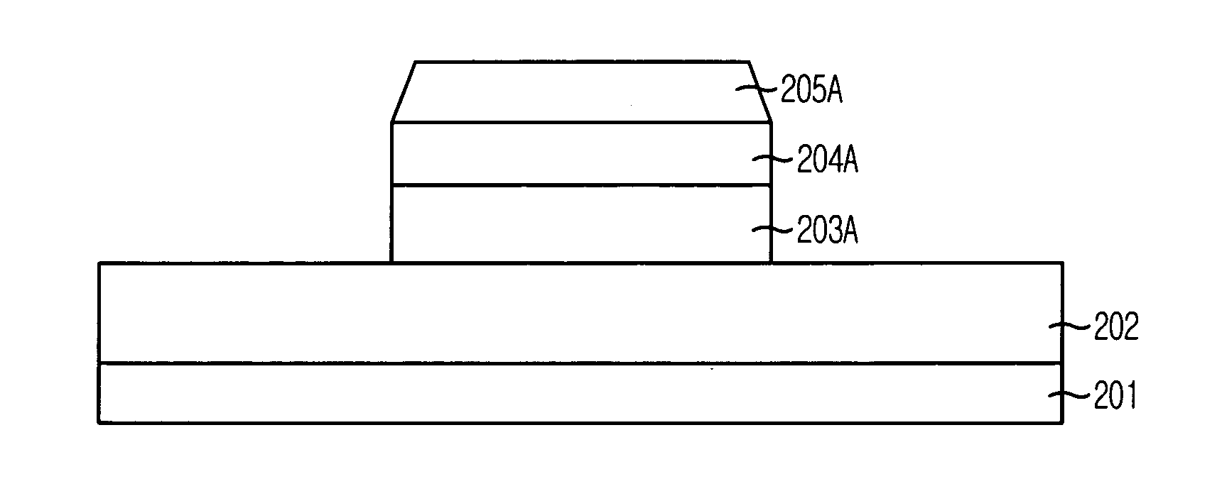
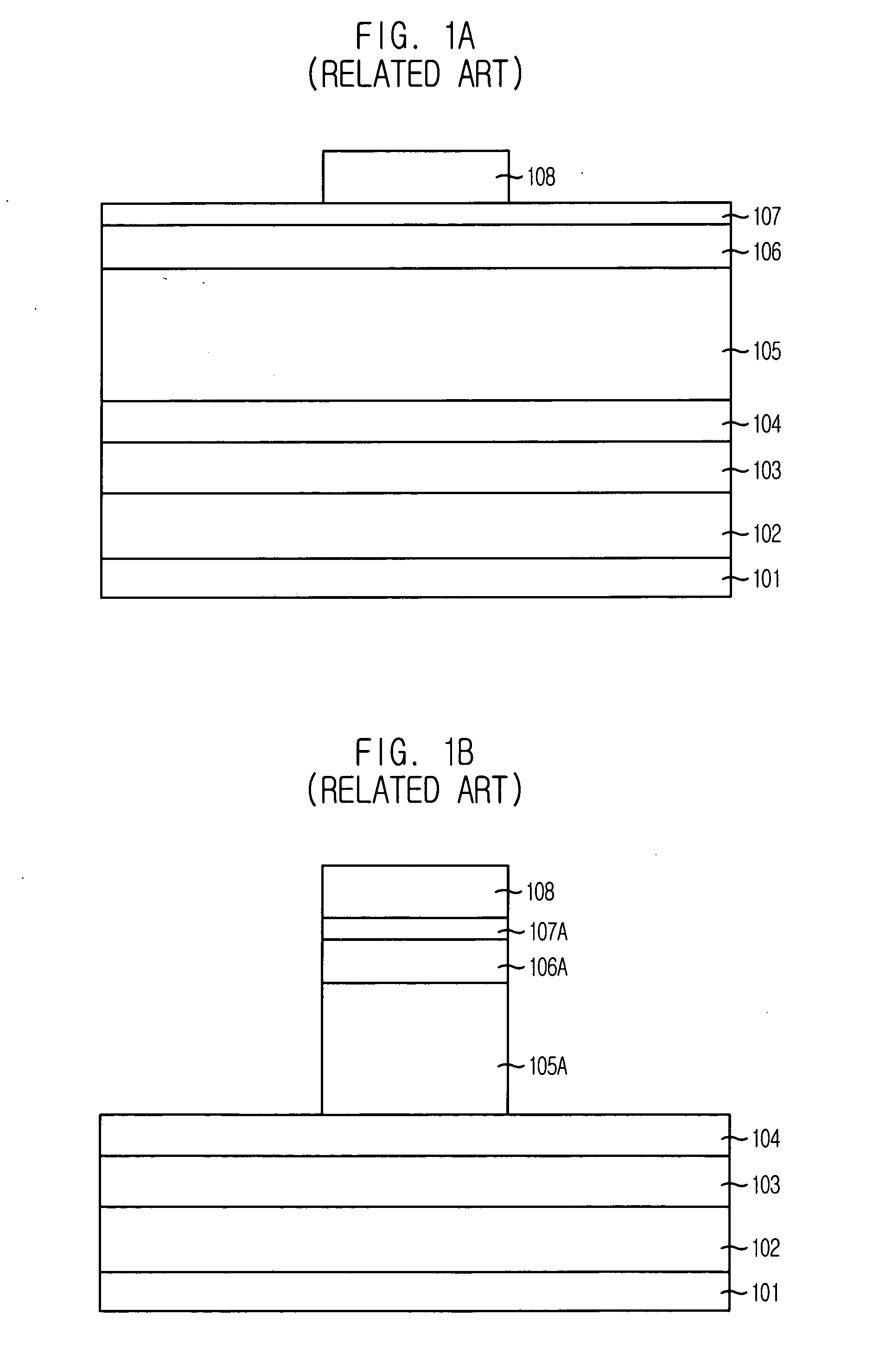
[0022]FIGS. 2A to 2C are cross-sectional views illustrating a method for fabricating a semiconductor device in accordance with a specific embodiment of the present invention.

[0023] As shown in FIG. 2A, a lower layer 202 is formed on a substrate 201.

[0024] Although not illustrated, the lower layer 202 is formed as follows.

[0025] First, a device isolation layer is formed on the substrate 201, which is divided into a cell region and a peripheral region, thereby defining an active region of the substrate 201. A gate insulation layer is formed on the substrate 201.

[0026] Next, a gate conductive layer and a hard mask nitride layer are formed on the gate insulation layer, and a photolithography process is performed thereon by using a gate mask pattern, thereby forming a gate structure.

[0027] Next, a lightly doped drain (LDD) ion-implan...


PUM


Abstract

A method for fabricating a semiconductor device is provided. The method includes sequentially forming etch target layers, a hard mask layer and an anti-reflective coating layer, selectively etching the anti-reflective coating layer and the hard mask layer using a gas generating polymers, thereby increasing a line width of a bottom portion of the hard mask layer due to the polymers, and etching the etch target layers using a patterned hard mask layer with the increased line width.

Description

FIELD OF THE INVENTION [0001] The present invention relates to a semiconductor device fabrication technology; and more particularly, to a method for fabricating a semiconductor device. DESCRIPTION OF RELATED ARTS [0002] A semiconductor device has been micronized and highly integrated, and a size of the semiconductor device has also been reduced. Accordingly, in case of a dynamic random access memory (DRAM), a channel length of a cell transistor and a contact size are also decreased. Due to the decreased channel length, a design margin for an internal pressure is reduced and thus, a plug concentration cannot get higher. Due to the decreased contact size, an actual contact area is also reduced, thereby increasing a contact resistance. Furthermore, a driving current is also reduced due to the above described reasons and accordingly, a device degradation phenomenon such as a tWR fail of a semiconductor device and degradation in a refresh property are generated. [0003]FIGS. 1A to 1C are ...

Claims


Application Information

Patent Timeline
IPC IPC(8): G03F1/00H01L21/302
CPCH01L21/32137H01L27/1052H01L27/105H01L21/32139H10B99/00H01L21/32H01L21/306
Inventor NAMLEE, KYUNG-WON
Owner SK HYNIX INC
Why Eureka
Try Eureka