

Method for manufacturing semiconductor device
- Summary
- Abstract
- Description
- Claims
- Application Information
AI Technical Summary
Benefits of technology
Problems solved by technology
Method used
Image

Examples
embodiment mode 1
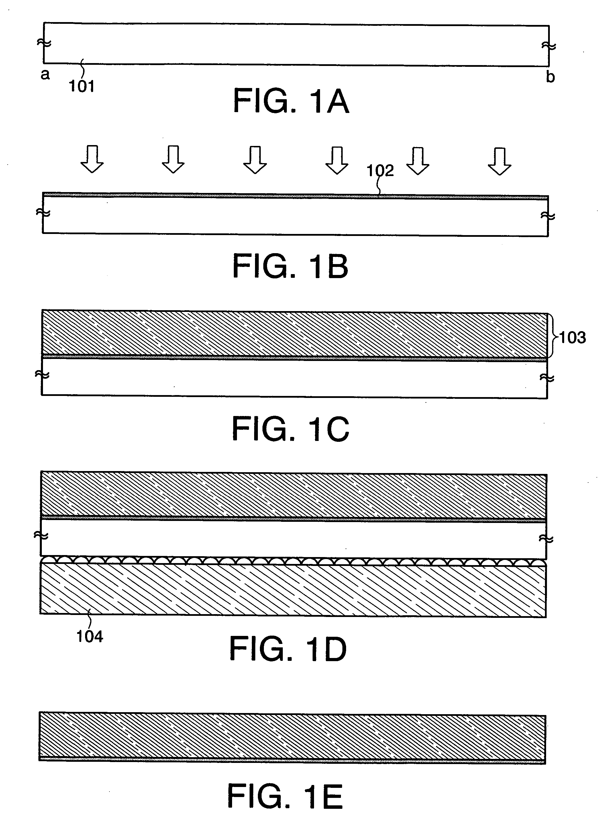
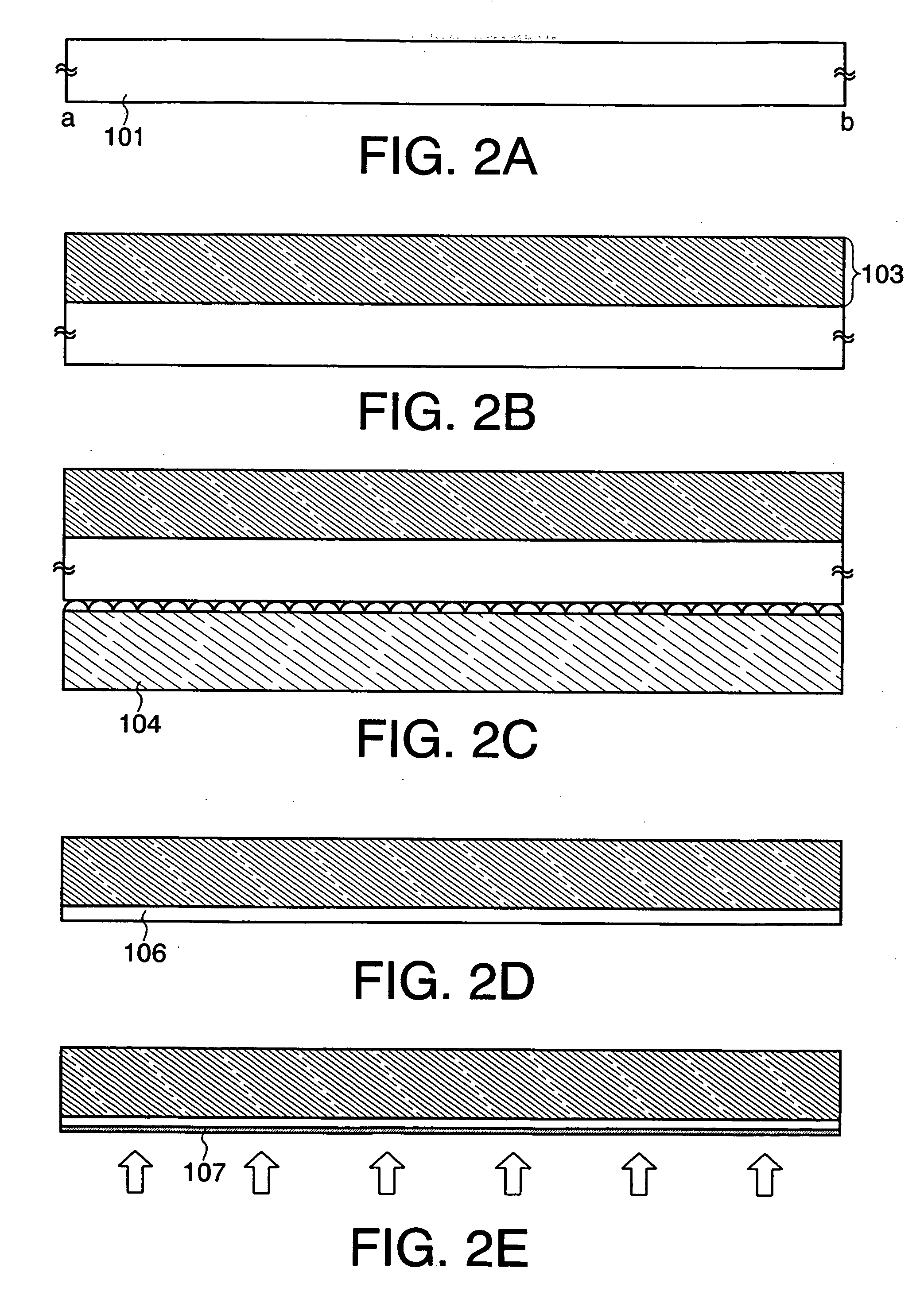
[0068] In this embodiment mode, an example of a method for manufacturing a semiconductor device of the present invention is explained with reference to FIGS. 3A to 4C. Initially, the above-described manufacturing method in FIGS. 1A to 1E is explained in more detail.
[0069] First, a substrate 201 is prepared, and a surface of the substrate 201 is washed using hydrofluoric acid (HF), or alkaline or pure water (FIG. 3A).
[0070] As the substrate 201, a glass substrate of barium borosilicate glass, aluminoborosilicate glass, or the like, a quartz substrate, a ceramic substrate, a metal substrate including stainless steel, a semiconductor substrate of Si or the like, or the like can be used. Note that the case of using a glass substrate as the substrate 201 is described here.
[0071] Next, nitriding treatment is performed on one side of the substrate 201 by plasma treatment to form a nitrided layer 202 (hereinafter also referred to as an “insulating film 202”) on the surface of the substra...
embodiment mode 2
[0102] In this embodiment mode, an example of an apparatus in the case of performing plasma treatment in the above embodiment mode is explained with reference to drawings.
[0103] A plasma treatment apparatus shown in FIG. 19A includes a plurality of treatment chambers capable of generating plasma, a common chamber for transferring a substrate to each chamber, and a load lock chamber for taking in or out the substrate. Thus, in the case of continuously performing formation of an insulating film, a conductive film, or a semiconductor film and plasma treatment thereof, a plasma treatment apparatus including a plurality of treatment chambers can be used. Note that FIG. 19A is a top plan view showing one exemplary structure of a plasma treatment apparatus described in this embodiment mode.
[0104] The plasma treatment apparatus shown as an illustrative example in FIG. 19A includes a first treatment chamber 311, a second treatment chamber 312, a third treatment chamber 313, a fourth treatm...
embodiment mode 3
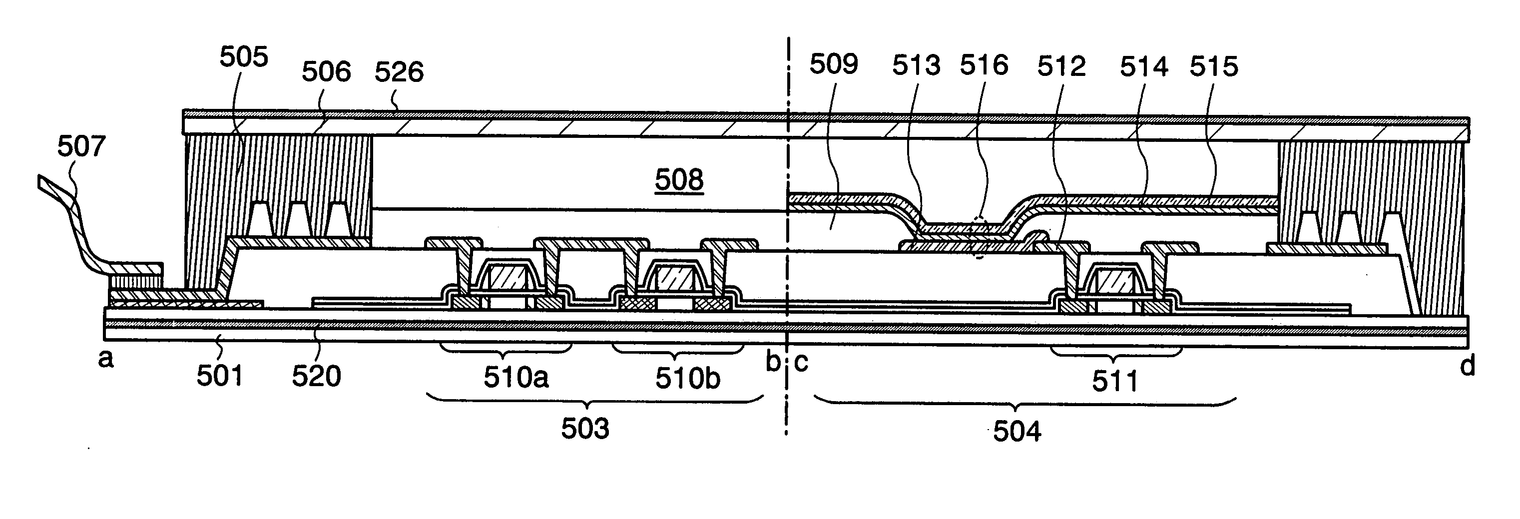
[0123] In this embodiment mode, a method for manufacturing a semiconductor device, which is different from that in the above embodiment modes, is explained with reference to drawings. Specifically, a method for manufacturing a semiconductor device of the present invention including a thin film transistor, a storage element, and an antenna is explained with reference to drawings.
[0124] First, one surface of a substrate 701 is subjected to plasma treatment in a nitrogen atmosphere to form a nitrided layer 702 (hereinafter also referred to as an insulating film 702). Subsequently, an insulating film 703 serving as a base film and an amorphous semiconductor film 704 (for example, a film containing amorphous silicon) are formed (FIG. 9A).
[0125] As the substrate 701, a glass substrate, a quartz substrate, a metal substrate, or a stainless steel substrate provided with an insulating film on one surface thereof, a heat-resistant plastic substrate which can withstand a processing temperatu...
PUM
 Abstract
Description
Claims
Application Information