High-brightness light emitting diode having reflective layer

a light-emitting diode, high-bright technology, applied in the direction of semiconductor devices, semiconductor/solid-state device details, electrical devices, etc., can solve the problems of reduced reflectivity, limited brightness, and improvement of the external quantum efficiency of leds, so as to achieve the effect of high-bright led structur

Active Publication Date: 2007-01-18
EPISTAR CORP
View PDF10 Cites 44 Cited by
  • Summary
  • Abstract
  • Description
  • Claims
  • Application Information

AI Technical Summary

Benefits of technology

[0011] The major objective of the present invention therefore is to provide a high brightness LED structure which obviates the foregoing shortcomings in resolving the substrate absorption problem.
[0013] The substrate could be either electrically conductive or non-electrically conductive. If non-electrically conductive substrate is used, the electrodes formed in the subsequent chip process have to be arranged in a planar fashion. If electrically conductive substrate is used, the electrodes could be arranged in a vertical or planar fashion. For planar electrode arrangement, the LED structure could have an optional insulating layer positioned between the substrate and the bottommost metallic layer for a superior insulating property.
[0014] The most significant characteristics of the present invention lie in the joint effect provided by the non-alloy ohmic contact layer and the first metallic layer in resolving the substrate absorption problem. The first metallic layer functions a reflective mirror and is made of a pure metal or a metal nitride for superior reflectivity. Since pure metal or metal nitride is used to substitute the conventional alloy reflective mirror so as to avoid the poor reflectivity from alloy metal or high annealing temperature, the non-alloy ohmic contact layer is interposed between the light generating structure and the first metallic layer so as to achieve the required low resistance electrical conduction. The material used for the non-alloy ohmic contact layer could be optically transparent or absorbing. For absorbing non-alloy ohmic contact layer, a number of recesses could be optionally formed along the bottom surface so as to reduce light absorption and to improve injection current distribution. For transparent non-alloy ohmic contact layer, recesses could still be formed for improving injection current distribution.
[0015] To further prevent the first metallic layer from intermixing with the non-alloy ohmic contact layer and the light generating structure, and to maintain the flatness of the reflective surface of the first metallic layer, an optically transparent and electrically conductive first dielectric layer could be interposed between the first metallic layer and the non-alloy ohmic contact layer. Additionally, to achieve superior bonding between the substrate and the first metallic layer, at least an additional metallic layer could be interposed between the first metallic layer and the substrate. Similarly, to prevent the additional metallic layer from intermixing with the first metallic layer and thereby compromising the reflectivity of the first metallic layer, a second dielectric layer could be interposed between the first metallic layers and the additional metallic layer.

Problems solved by technology

However, the DBRs provide high reflectivity only for normal incident lights and the reflectivity decreases as the lights' incident angle increases.
The improvement to the LED's external quantum efficiency and brightness is therefore limited.
However, the problem with the approach using transparent substrate is that its wafer-bonding process requires to be operated under a high annealing temperature over an extended period of time, which would cause redistribution of doping profile and degrade the LED's performance.
The problem with the approach using mirror is that the mirror's reflective surface is directly involved in the bonding interface during the wafer-bonding process, which would lead to roughness of the reflective surface or reactions and contaminations to the mirror's reflective surface.
However, alloy material AuBe possesses inferior reflectivity and thereby limits the brightness improvement of the LED.
The alloy process, which usually requires a high annealing temperature, would also compromise the surface flatness of the reflective mirror and degrade its reflectivity.
The disclosed structure has rather complicated fabrication process, and therefore a high production cost.
The alloy metal mesh requires a high temperature alloy process, and etching the alloy metal to form mesh is also very difficult to control.
In addition, the thickness of the alloy metal requires special attention.
If the alloy metal is too thin, the ohmic contact between the alloy metal and the light generating structure is inferior; if the alloy metal is too thick, the wafer bonding process couldn't achieve a strong bonding.

Method used


Image

  • High-brightness light emitting diode having reflective layer
  • High-brightness light emitting diode having reflective layer
  • High-brightness light emitting diode having reflective layer

Examples


Embodiment Construction

[0027] The following descriptions are exemplary embodiments only, and are not intended to limit the scope, applicability, or configuration of the invention in any way. Rather, the following description provides a convenient illustration for implementing exemplary embodiments of the invention. Various changes to the described embodiments may be made in the function and arrangement of the elements described without departing from the scope of the invention as set forth in the appended claims.

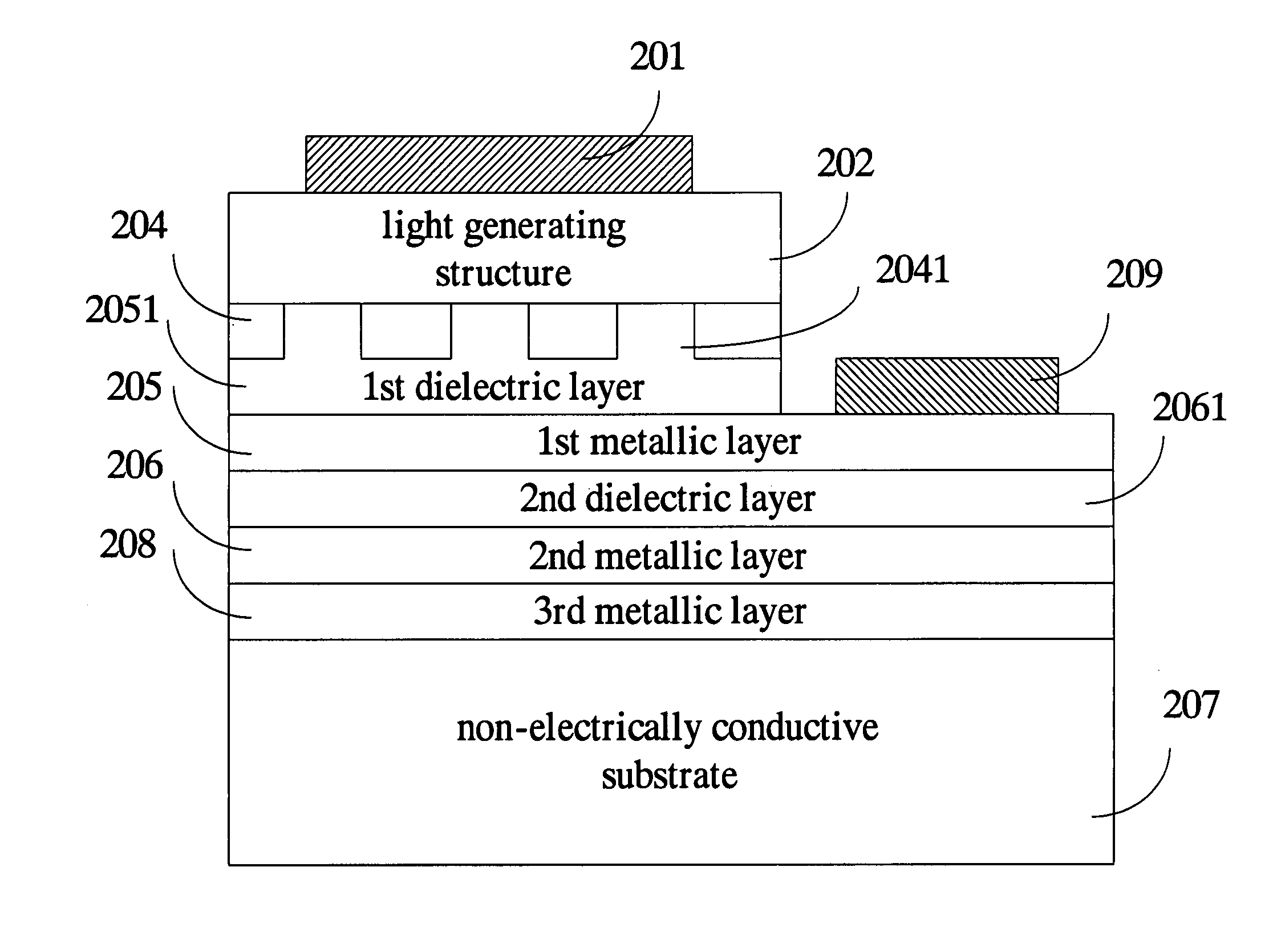
[0028]FIG. 2a is a schematic sectional view showing the structure of an LED according to a first embodiment of the present invention. As illustrated, the LED structure contains a light generating structure 202. The light generating structure 202 includes active p-n junction layers for generating lights in response to the conduction of current. The light generating structure 202 usually contains, but not limited to, a number of III-V compound semiconductor layers. The exact details of the light ge...


PUM

PropertyMeasurementUnit
metallicaaaaaaaaaa
transparentaaaaaaaaaa
electrically conductiveaaaaaaaaaa

Abstract

An LED structure is disclosed herein, which comprises, sequentially arranged in the following order, a light generating structure, a non-alloy ohmic contact layer, a metallic layer, and a substrate. As a reflecting mirror, the metallic layer is made of a pure metal or a metal nitride for achieving superior reflectivity. The non-alloy ohmic contact layer is interposed between the metallic layer and the light generating structure so as to achieve the required ohmic contact. To prevent the metallic layer from intermixing with the non-alloy ohmic contact layer and to maintain the flatness of the reflective surface of the first metallic layer, an optional dielectric layer is interposed between the metallic layer and the non-alloy ohmic contact layer.

Description

BACKGROUND OF THE INVENTION [0001] 1. Field of the Invention [0002] The present invention generally relates to light emitting diodes, and more particularly to a light emitting diode having a reflective layer to avoid light absorption by the diode's substrate. [0003] 2. The Prior Arts [0004]FIG. 1a is a schematic sectional view showing a typical structure of a conventional light emitting diode (LED). As illustrated, the LED 100 contains a semiconductor substrate 103 and a light generating structure 102 on top of the substrate 103, and two ohmic contact electrodes 109 and 101 formed on the other side of the substrate 103 and on top of the light generating structure 102 respectively. [0005] The light generating structure 102 is often made of layers of aluminum-bearing III-V compound semiconductors, such as AlGaAs for infrared and red lights, AlGaInP for yellow-green, yellow, amber, and red lights. The substrate 103 is usually made of gallium arsenide (GaAs) which has a matching lattice...

Claims


Application Information

Patent Timeline
Patent Type & Authority Applications(United States)
IPC IPC(8): H01L29/22H01L21/28H01L33/00H01L33/38H01L33/40
CPCH01L33/0079H01L33/405H01L33/387H01L33/0093
Inventor LIU, JIN-HSIANGWANG, HUI-HENGLIN, KUN-CHUAN
Owner EPISTAR CORP
Why Eureka
Try Eureka