Semiconductor device integrated with opto-electric component and method for fabricating the same

a technology of opto-electric components and semiconductors, which is applied in the direction of optical elements, instruments, optical waveguide light guides, etc., can solve the problems of increasing the conductivity, unable to achieve further conductivity, and the inability to increase the signal transmission rate by increasing the conductivity, so as to improve the aligning precision, shorten the conduction path, and reduce the loss of signal transmission

Active Publication Date: 2007-03-01
PHOENIX PRECISION TECH CORP
View PDF10 Cites 6 Cited by
  • Summary
  • Abstract
  • Description
  • Claims
  • Application Information

AI Technical Summary

Benefits of technology

[0017] Another objective of the present invention is to provide asemiconductor device integrated with opto-electric component and method for fabricating the same, to increase the aligning precision when circuits bond to components by applying the flip chip bonding.
[0018] A further objective of the present invention is to provide asemiconductor device integrated with opto-electric component and method for fabricating the same, to lower the signal transmission loss, shorten the conduction path, reduce the noise and increase the electric performance.
[0030] Therefore, the present invention of a semiconductor device integrated with opto-electric component and method for fabricating the same is to form an opening on a wafer with a plurality of optical transmitter / receiver components to expose the single layer or the multi-layer circuit structure of the optical active area of the optical transmitter / receiver components. To allow the circuit of the single layer or the multi-layer circuit structures to be electrically connected to the connecting pads of the optical transmitter / receiver components directly in order to improve the bonding alignment between the circuit and the connecting pads of the optical transmitter / receiver components. Afterwards, performing a routing process formed a plurality of integrated devices with single optical transmitter / receiver component to achieve the chip packaging of the optical transmitter / receiver component, therefore leads to a reduced product's package volume to form an integrated device meeting the requirement of the small and lightweight electronic devices, and therewith, lowers the signal transmission loss, shortens the transmission path and reduces the noise to improve the optoelectronics' quality by the integration of the optoelectronics.

Problems solved by technology

The straightest way to increase the semiconductor's processing rate is to increase the utilization ratio, but facing bottlenecks such as heatsink for high power, delay of signal time and electric magnetic interruption (EMI) when the data transmission is above Gb / s, which makes the fabrication of the higher performance semiconductor more difficult.
Especially when the copper circuit is conventionally used as a carrier for data transmission, with the limitation of this material's natural conductivity, the achieved conductivity cannot be increased further, therefore the signal transmission rate cannot be increased by increasing the conductivity.
In addition, the metallic circuit structure for signal transmission is easy to have interruption from the outside noise or interference from the inner circuit, results in signal transmission error due to the interruption and interference during the signal transmission process; therefore, some protection methods are required for the signal transmission structure to prevent the interruption and interference occur to affect the signal, especially obvious in the high frequency transmission.
The protection methods have increased some difficulties and extra structure design for the circuit design, results in increasing in the design cost and the fabrication cost, and therefore, the present condition is hard to make a breakthrough.
Moreover, the conventional signal transmission method is an analogue signal transmission method using electricity flowing through the conductor, but the signal processing methods inside the circuits nowadays mostly are digital processing; therefore a distortion may occur after conversion during the transmission process.
An automatic placing movement, like the conventional insertion movement when inserting electronic components into a circuit board, completes the fabrication process of placing the optical fiber 13 into the groove 12a; therefore the speed of the fabrication is slow, and cannot achieve the rapid production purpose.
Moreover, the optical fiber 13 needs to be cut first according to the corresponding groove 12a length, and then places the optical fiber 13 into the groove 12a, which adds another process in the fabrication, therefore increases the fabrication difficulty; and the optical fiber 13 has different lengths, thereof increases the fabrication assorting difficulties, leads to the addition of the whole fabrication's process and complexity, and consequently increases the fabrication cost.
The optical fiber 13 and the circuit board have different fabrication structure, thus needs to be fabricated by another independent fabrication process and increases the whole fabrication's difficulty; and to integrate the two different fabrication products increase difficulty as well, thus cannot achieve the mass production purpose to lower the fabrication cost.
Thus, the increasing fabrication difficulty and cost due to optical fiber 13 has to be embedded in the saturated layer 12, and further, failing to meet the high density wiring requirements, has become problems for industries desired to be resolved.
In addition, when using the optical fiber connector for the straight connection, because of the poor performance of the automatic production, a high accuracy alignment equipment is applied for the optical signal transmission and the alignment process is done by hand; this process not only increases the fabrication cost, but also reduces the productivity.
Beside, the use of optics for data transmission of the prior art comprises mainly by the signal processing components, such as the optical fiber, optical connector, optical / electrical converter and electrical / optical converter, thereby complete the digital data transmission; but the high accuracy optical alignment and the system are huge in dimension, which is a disadvantage in the current small and lightweight designing trend.

Method used


Image

  • Semiconductor device integrated with opto-electric component and method for fabricating the same
  • Semiconductor device integrated with opto-electric component and method for fabricating the same
  • Semiconductor device integrated with opto-electric component and method for fabricating the same

Examples


Embodiment Construction

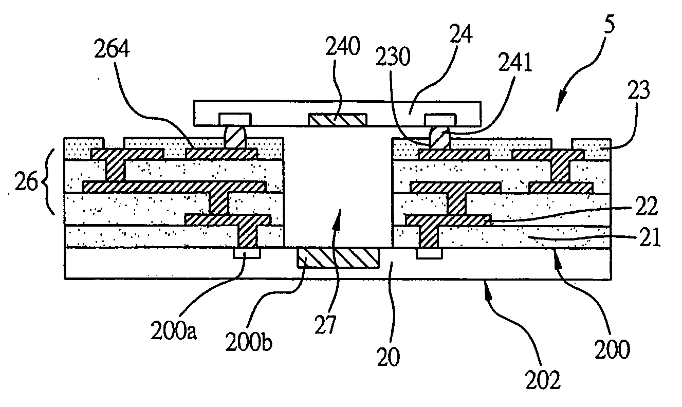
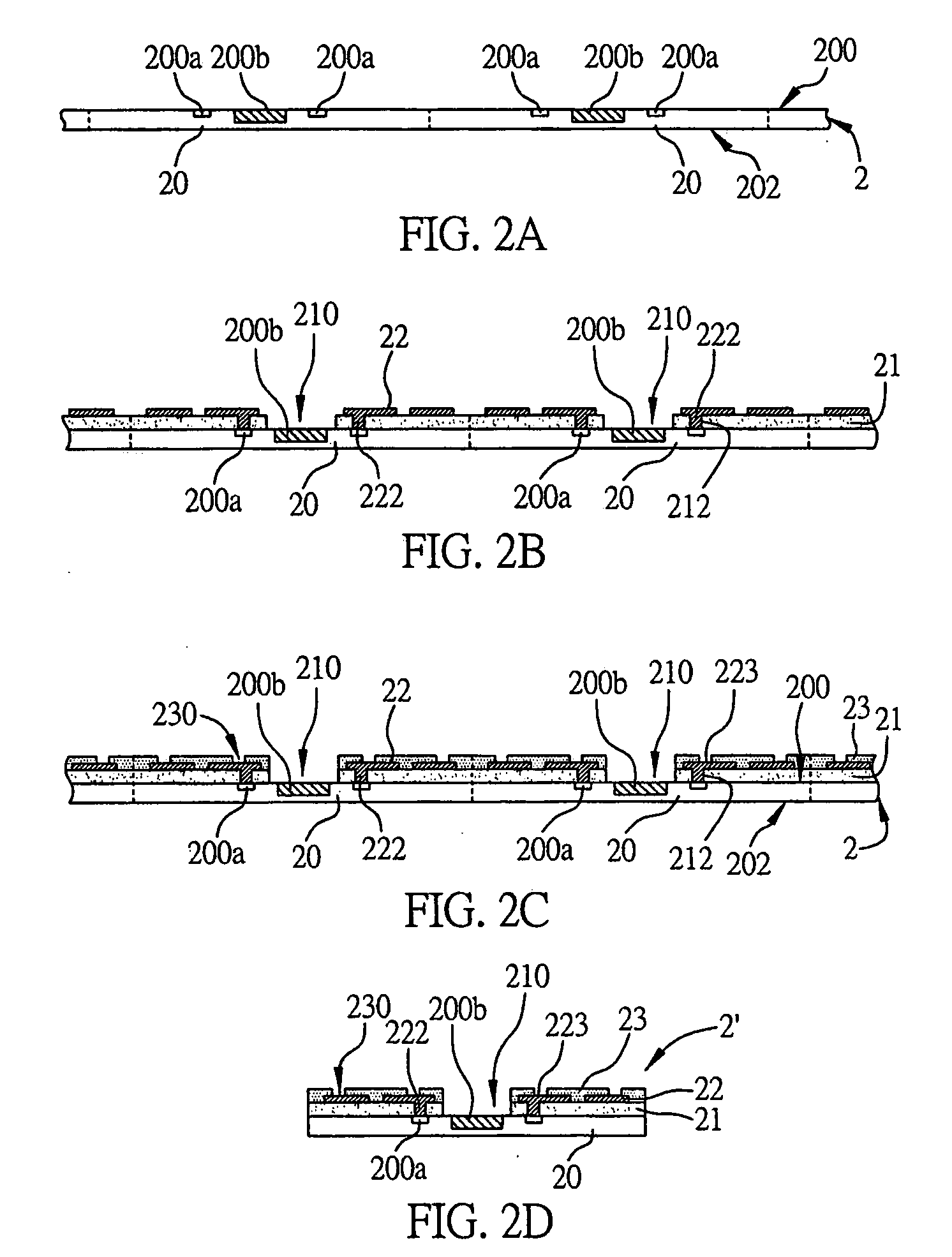
[0037]FIGS. 2A to 2D show the first preferred embodiment's fabrication flowchart of the present invention of the semiconductor device integrated with opto-electric component. Please notice that all the diagrams are simplified schematic diagrams only, and only used to represent the fabrication process of the present invention. Furthermore, the diagrams only show the components relating to the present invention, and the showing components are not in their actual condition when operation; the design of the components' number, shape and size is selective in actual operation and the components can be arranged in a more complex way.

[0038] As shown in FIG. 2A, first a semiconductor wafer 2 with a plurality of optical transmitter / receiver components 20 is provided, each of the optical transmitter / receiver components 20 having an active surface 200 and a non-active surface 202 opposites to the active surface 200, wherein a plurality of connecting pads 200a and an optical active area 200b ar...


PUM


Abstract

A semiconductor device integrated with opto-electric component and method for fabricating the same provides a wafer with a plurality of optical transmitter / receiver components, and each of the optical transmitter / receiver components having an active surface and an opposite non-active surface, wherein a plurality of connecting pads and an optical active area are formed on the active surface; a dielectric layer and a circuit layer formed on the active surface, wherein the circuit layer is electrically connected to the connecting pads through electrical conductive structures formed in the dielectric layer; and an opening formed through the dielectric layer to expose the optical active area on the active surface; then an insulating layer is further formed on the circuit layer. By performing a routing process on the wafer to form a plurality of integrated devices with the optical transmitter / receiver components and circuit structures to fulfill the small and lightweight requirements of the electronic device.

Description

CROSS-REFERENCE TO RELATED APPLICATION [0001] This application claims benefit under 35 USC 119 to Taiwan Application No. 094129453, filed Aug. 29, 2005. FIELD OF THE INVENTION [0002] The present invention relates to a semiconductor device integrated with opto-electric component and methods for fabricating the same, and more particularly, to a semiconductor device integrated with an optical transmitter / receiver chip and a circuit structure and a method for fabricating the same. BACKGROUND OF THE INVENTION [0003] The development of semiconductor technology improves day by day rapidly, besides mainly focusing on the tiny packaging of the model, nowadays the data storage capacity is increasing gradually also. Therefore, with the increasing data quantity, the least time taken to process the same quantity data shows a higher efficiency in data processing. The straightest way to increase the semiconductor's processing rate is to increase the utilization ratio, but facing bottlenecks such a...

Claims


Application Information

Patent Timeline
Patent Type & Authority Applications(United States)
IPC IPC(8): G02B6/12
CPCH01L31/0203H01L25/167H01L24/05H01L2224/02379H01L2224/05001H01L2224/05008H01L2224/05024H01L2224/05548H01L2224/05571H01L2224/16225H01L2924/00014H01L2224/05599H01L2224/05099
Inventor HSU, SHIH-PING
Owner PHOENIX PRECISION TECH CORP
Why Eureka
Try Eureka