[0008] The photo-electric conversion parts in a CCD
solid state imaging device are formed in valleys between large-height transfer electrodes on a
semiconductor substrate. Of the transfer
electrode array, both the upper surfaces and the side wall surfaces are covered with the light-shielding layer. Therefore, if the light-shielding layer is larger in thickness, the side wall surfaces of the transfer
electrode array are bulged more accordingly, and the width of the valleys between the transfer electrodes becomes smaller. As a result, the aperture area of the photo-electric conversion parts is reduced, leading to a lower sensitivity. This is the reason for the fact that a light-shielding layer is more advantageous as its thickness is smaller. In addition, a reduction in the thickness of the light-shielding layer is important also for pursuing a further
miniaturization of the solid state imaging device. Accordingly, it is desired to use a
film material with a higher
extinction coefficient as the material of the light-shielding layer.
[0009] As a material further higher than
tungsten in
extinction coefficient, ruthenium and
iridium are known. For light with a
wavelength region in the vicinity of 700 nm,
tungsten has an extinction coefficient of 2.78 to 2.91, whereas ruthenium has 4.45 to 4.22 and iridium has 4.81 to 4.92. Thus, ruthenium and iridium are higher than
tungsten in extinction coefficient by about 60%; therefore, when ruthenium or iridium is used, the thickness of the light-shielding layer can be reduced by about 60%, as compared with the case of using tungsten.
[0010] However, in the CCD solid state imaging device, after the formation of the light-shielding layer, a transparent layer composed of
boron phosphorus silicate glass (BPSG) or
phosphorus silicate glass (PSG) is formed thereon, for the purpose of forming a
waveguide path or a lens. The BPSG film and the PSG film are transparent
layers which show an oxidizing property at the time of film formation; particularly, these films show a strong oxidizing property in a heating reflow step included in the film forming process. On the other hand, ruthenium and iridium are materials liable to be oxidized; therefore, when the light-shielding layer is formed by use of ruthenium or iridium, the metallic material will be easily oxidized at the time of forming the transparent layer thereon. Particularly, when ruthenium (Ru) is converted into its
oxide (RuOx), the extinction coefficient is lowered as compared with that of the elemental ruthenium, so that it becomes difficult to obtain the expected light shielding performance. In addition, part of ruthenium may be converted into volatile
ruthenium tetroxide (RuO4) and be evaporated, with also leads to local
thinning of the light-shielding layer, accompanied by a lowering in light shielding performance at the thinned portion and a worsening of the smear characteristic.
[0014] Thus, there is another need to ensure that the misalignment in patterning of a
photoresist mask can be absorbed, without forming any edge portion projecting largely from the lower end of a side wall surface of a transfer
electrode array toward a photo-electric conversion part at
peripheral edges of the openings formed in a light-shielding layer in correspondence with the photo-electric conversion parts, and that the reduction in the aperture area of the photo-electric conversion parts and the lowering of sensitivity can be thereby obviated, in manufacturing a solid state imaging device in which the photo-electric conversion portion array including a plurality of photo-electric conversion parts and the transfer electrode array including a plurality of transfer electrodes are provided in parallel to each other, and the upper surfaces and side wall surfaces of the transfer electrode array are covered with the light-shielding layer provided with the openings corresponding to the photo-electric conversion parts.
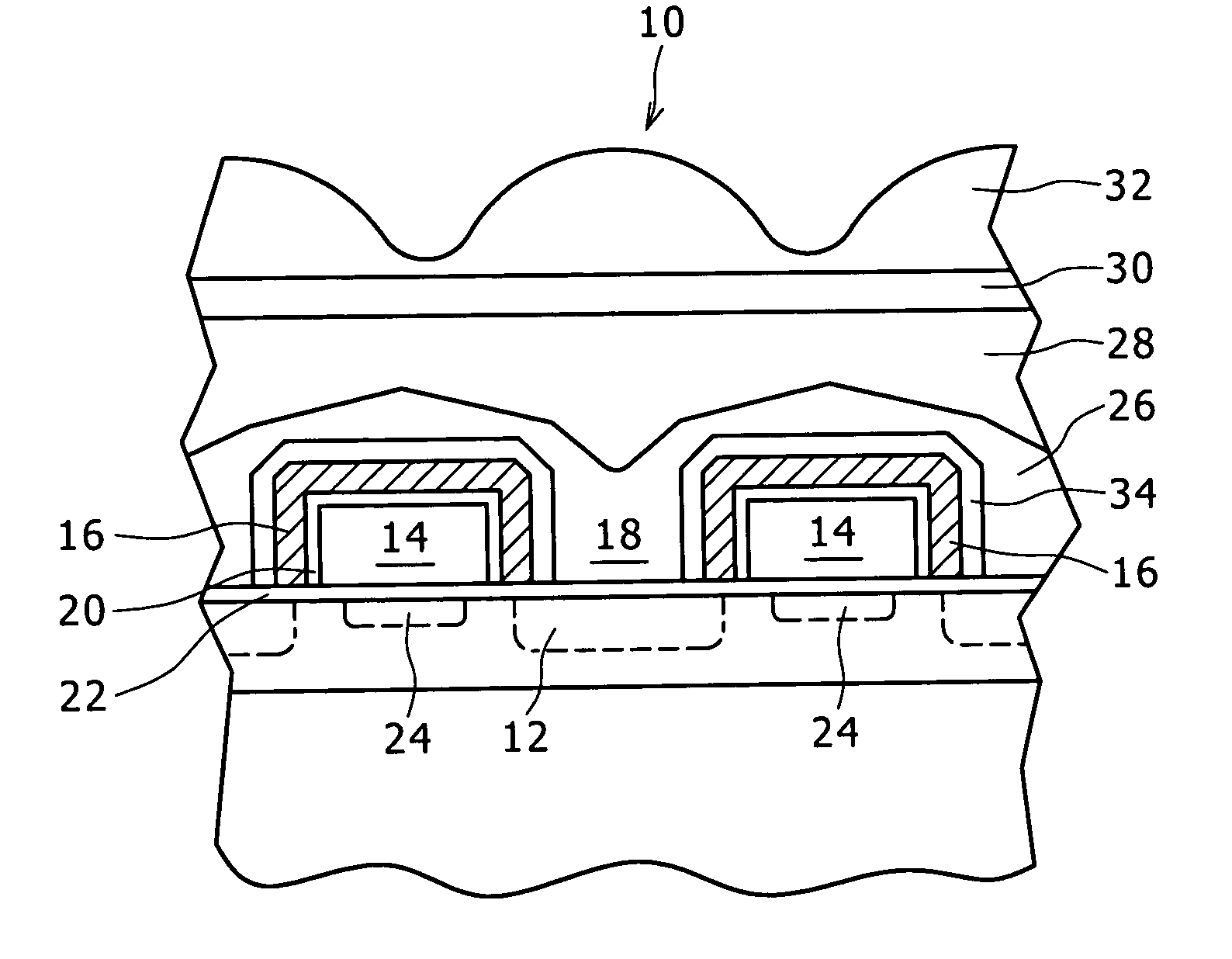
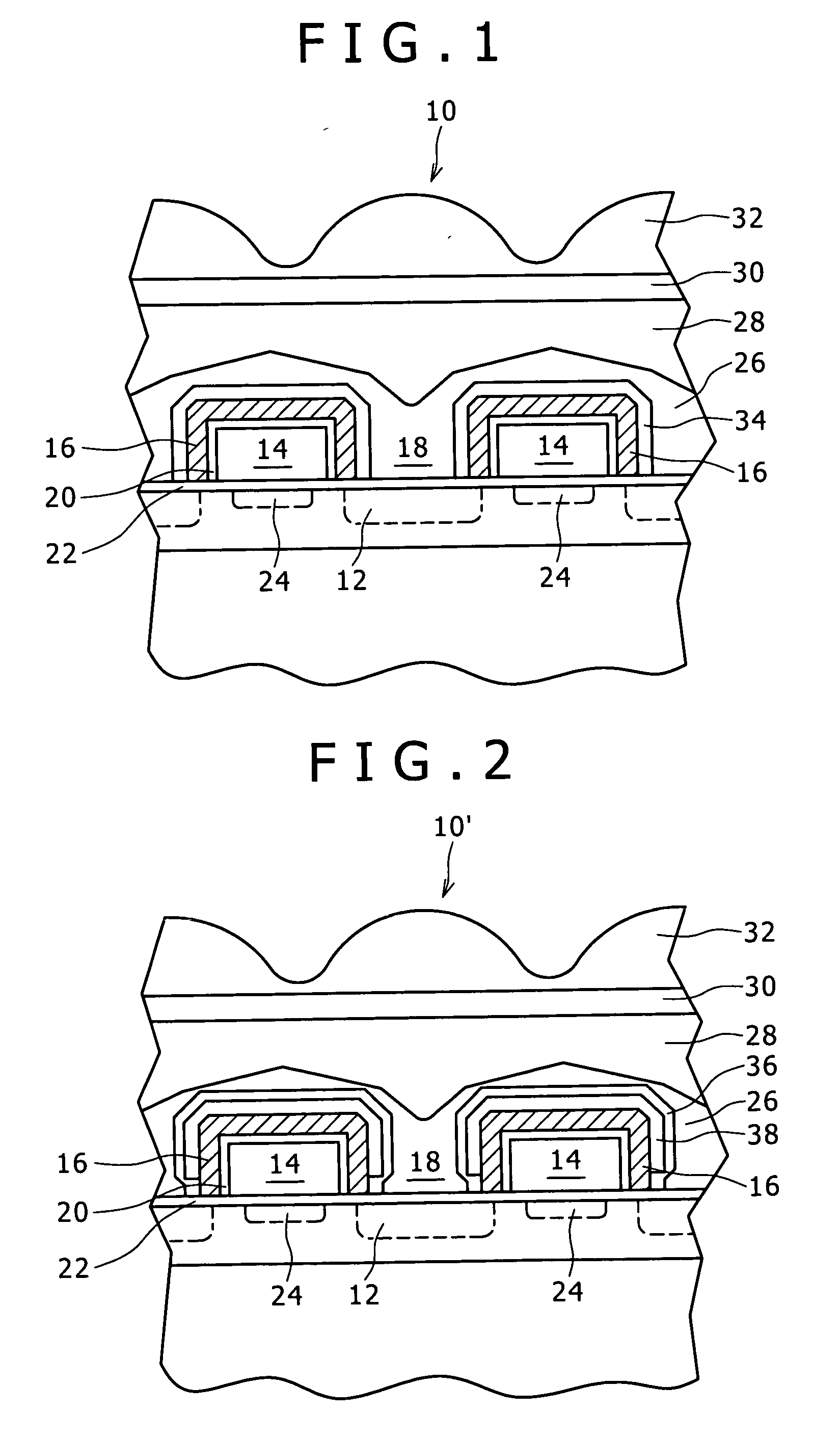
[0024] According to the present invention, the light-shielding layer covering the upper surfaces and side wall surfaces of the transfer electrode array are completely isolated by the anti-oxidizing
passivation layer from the transparent layer showing an oxidizing property at the time of film formation. Therefore, those materials which have hitherto not been able to be used as a light-shielding layer material notwithstanding their high extinction coefficients because they are susceptible to oxidation can be used to form a light-shielding layer, whereby the thickness of the light-shielding layer can be largely reduced.
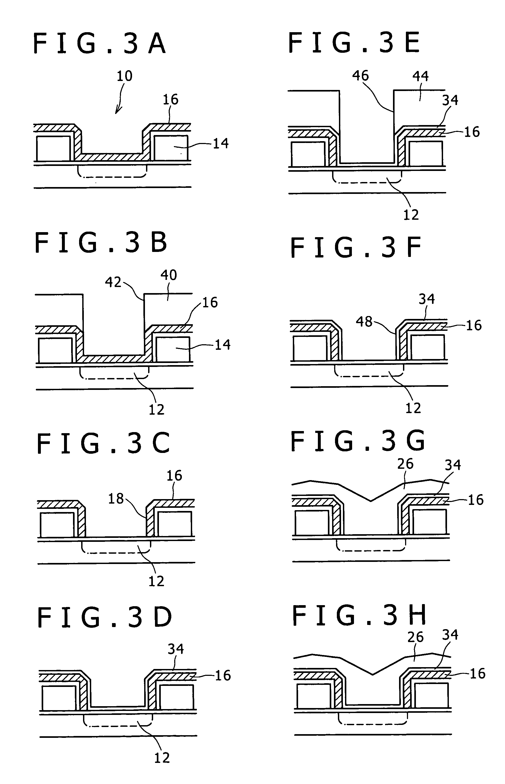
[0025] In addition, according to the present invention, in forming the light-shielding layer provided with the openings corresponding to the photo-electric conversion parts, a method of forming the openings by
anisotropic etching using a
photoresist mask as in the related-art method is not adopted; instead, a
hard mask is first formed by
anisotropic etching using a
photoresist mask, and then the openings corresponding to the photo-electric conversion parts are formed in the light-shielding layer by
anisotropic etching using the
hard mask. Therefore, the misalignment in patterning of the photoresist mask in the manufacturing process can be absorbed by the thickness of the
hard mask, without forming edge portions projecting largely from the lower ends of side wall surfaces of the transfer electrode array toward the photo-electric conversion parts at the
peripheral edges of the openings formed in the light-shielding layer in correspondence with the photo-electric conversion parts. As a result, the reduction in the aperture area of the photo-electric conversion parts and the lowering in sensitivity can be obviated.

