Semiconductor device, manufacturing method thereof, liquid crystal display device, RFID tag, light emitting device, and electronic device

Inactive Publication Date: 2007-03-29
SEMICON ENERGY LAB CO LTD
View PDF12 Cites 28 Cited by
  • Summary
  • Abstract
  • Description
  • Claims
  • Application Information

AI Technical Summary

Benefits of technology

[0018] As described above, the present invention can provide a semiconductor device in which characteristics of the semiconductor device are improved by thinning a gate insulating film

Problems solved by technology

However, when an insulating film having a high dielectric constant is us

Method used


Image

  • Semiconductor device, manufacturing method thereof, liquid crystal display device, RFID tag, light emitting device, and electronic device
  • Semiconductor device, manufacturing method thereof, liquid crystal display device, RFID tag, light emitting device, and electronic device
  • Semiconductor device, manufacturing method thereof, liquid crystal display device, RFID tag, light emitting device, and electronic device

Examples


embodiment mode 1

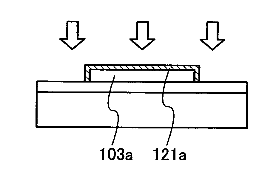
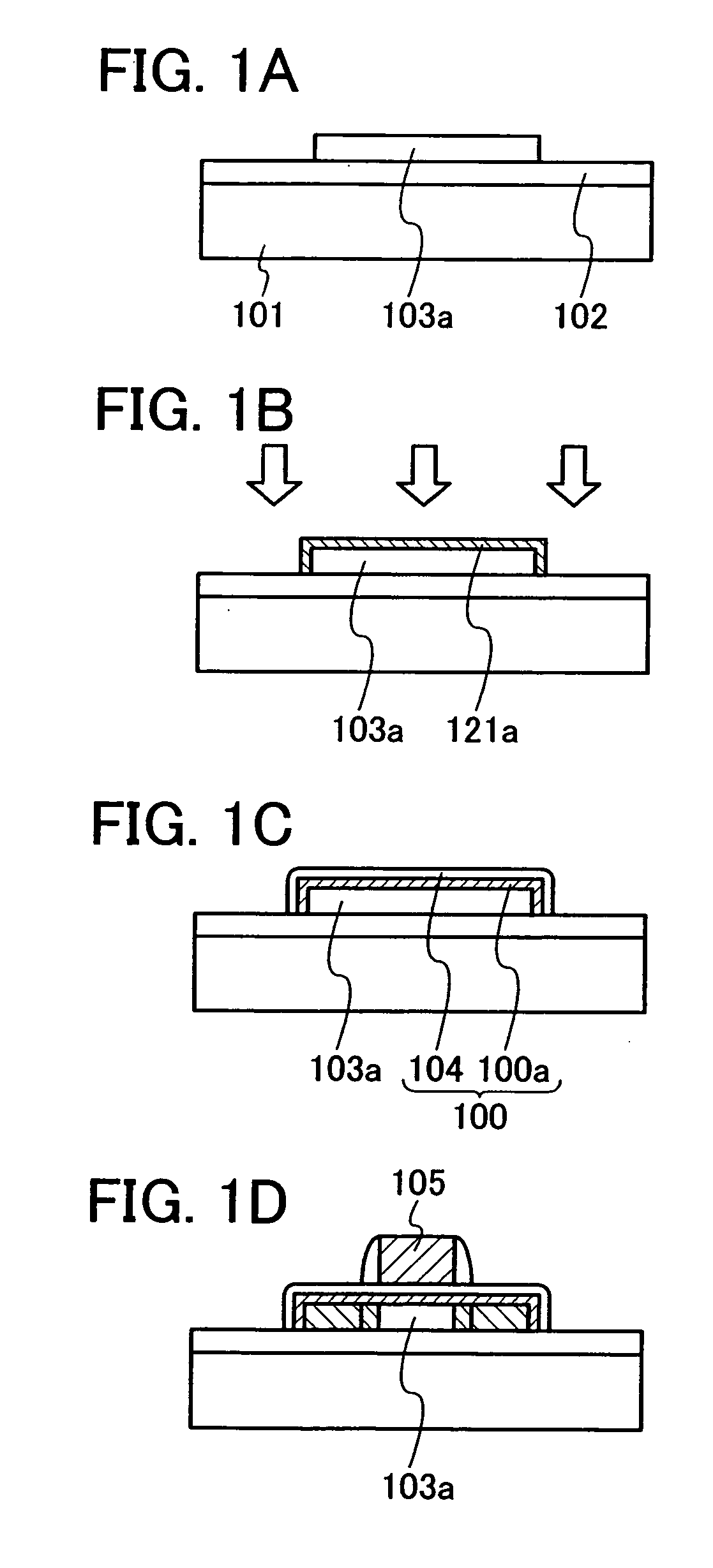
[0049]FIGS. 1A to 1D are cross-sectional views each showing a manufacturing method of a semiconductor device according to Embodiment Mode 1 of the present invention.

[0050] First, an island-shaped polycrystalline semiconductor film (e.g. polysilicon film) 103a is formed over a glass substrate 101 (FIG. 1A). It is preferable to use a silicon film or a silicon germanium film as the semiconductor film. The same also applies to other embodiment modes. The island-shaped polysilicon film 103a can be provided as follows: An amorphous semiconductor film such as an amorphous silicon film having a thickness of approximately 30 to 200 nm is formed over an insulating film 102, which is formed over a glass substrate 101 in advance, by a sputtering method, an LPCVD method, a plasma CVD method, or the like; dehydrogenation is performed to the amorphous silicon film by heating at temperatures of 450 to 500° C.; the amorphous silicon film is crystallized to form a polysilicon film; and the polysilic...

embodiment mode 2

[0056] A manufacturing method of a semiconductor device according to Embodiment Mode 2 of the present invention is different from the method of Embodiment Mode 1 in that: After an aluminum film is formed over an island-shaped polycrystalline semiconductor film (e.g. polysilicon film), plasma treatment is performed to the aluminum film in an atmosphere containing nitrogen to form an aluminum nitride film which is a metal nitride film; plasma treatment is further performed to the aluminum nitride film in an atmosphere containing oxygen to form an aluminum oxide film (containing nitrogen) which is a metal oxide film containing nitrogen; and then, plasma treatment is performed to the aluminum oxide film in an atmosphere containing oxygen to form a silicon oxide film having a thickness of approximately 0.5 to 1 nm between the polysilicon film and the aluminum oxide film. When oxidizing treatment is performed after nitriding treatment as described above, the metal nitride film is almost o...

embodiment mode 3

[0059] A manufacturing method of a semiconductor device according to Embodiment Mode 3 of the present invention is different from the method of Embodiment Mode 1 in that: After an aluminum film is formed over an island-shaped polycrystalline semiconductor film (e.g. polysilicon film), plasma treatment is performed to the aluminum film in an atmosphere containing oxygen to form an aluminum oxide film which is a metal oxide film; plasma treatment is further performed to the aluminum oxide film in an atmosphere containing oxygen to form a silicon oxide film having a thickness of approximately 0.5 to 1 nm between the polysilicon film and the aluminum oxide film; and then, plasma treatment is performed to the aluminum oxide film in an atmosphere containing nitrogen to form an aluminum oxide film (containing nitrogen) which is a metal oxide film containing nitrogen. The nitriding treatment here is performed to a portion which is 1 to 2 nm deep from the surface of the aluminum oxide film, ...


PUM

PropertyMeasurementUnit
Thicknessaaaaaaaaaa
Thicknessaaaaaaaaaa

Abstract

There is provided a semiconductor device, in which characteristics of the semiconductor device are improved by thinning a gate insulating film and a leak current can be reduced, and a manufacturing method thereof. An aluminum film which is a metal film is formed over a polycrystalline semiconductor film, and plasma oxidizing treatment is performed to the aluminum film, whereby an aluminum oxide film is formed by oxidizing the aluminum film, and a silicon oxide film is formed between the polycrystalline semiconductor film and the aluminum oxide film.

Description

BACKGROUND OF THE INVENTION [0001] 1. Field of the Invention [0002] The present invention relates to a semiconductor device, a manufacturing method of the semiconductor device, a liquid crystal display device, an RFID (Radio Frequency Identification) tag, a light emitting device, and an electronic device. In particular, the present invention relates to a semiconductor device in which characteristics of the semiconductor device are improved by thinning a gate insulating film and a leak current can be reduced, a manufacturing method of the semiconductor device, a liquid crystal display device, an RFID tag, a light emitting device, and an electronic device. [0003] 2. Description of the Related Art [0004] When a semiconductor device is miniaturized, a thickness of a gate insulating film is thinned by scaling law. In a conventional semiconductor device formed over a single crystal silicon substrate, a tunnel current is generated when a gate insulating film is thin. In order to overcome a...

Claims


Application Information

Patent Timeline
IPC IPC(8): H01L21/31
CPCC23C8/36C23C14/028C23C14/16C23C14/5826C23C14/5853C23C14/586H01L29/4908C23C16/20C23C16/56H01L21/31683H01L27/1214H01L27/13C23C16/0263H01L27/127H01L27/124H01L27/1251H01L21/02252H01L21/02244H01L21/02326H01L21/02247H01L21/02175H01L21/0234
Inventor KAKEHATA, TETSUYA
Owner SEMICON ENERGY LAB CO LTD
Why Eureka
Try Eureka