Method for forming metal wiring structure

Active Publication Date: 2007-04-12
ASM JAPAN
View PDF16 Cites 393 Cited by
  • Summary
  • Abstract
  • Description
  • Claims
  • Application Information

AI Technical Summary

Benefits of technology

[0034] In another aspect, in any one of the foregoing methods, the insulating layer may be porous and have pores, which method further comprises, prior to step (ii), (a) forming a pore-sealing layer to block pores at least on an exposed surface of the insulating layer; and (b) removing a portion of the pore-sealing layer, if any, formed on an exposed surface of the wiring layer, wherein the exposed surface of the insulating layer in step (ii) on which the terminal containing N and H is introduced is comprised of a sur

Problems solved by technology

However, it is difficult to form a thin Ru film directly on an interlayer insulation film by means of atomic-layer deposition.
Forming a smooth thin film on an insulation layer is particularly difficult, because a porous insulation film is generally used to keep the dielectric constant low.
In this case, however, smoothness of the barrier fi

Method used


Image

  • Method for forming metal wiring structure
  • Method for forming metal wiring structure
  • Method for forming metal wiring structure

Examples


example 1

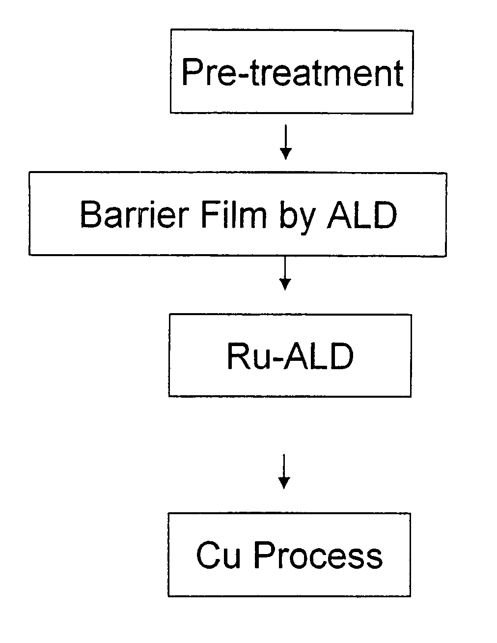
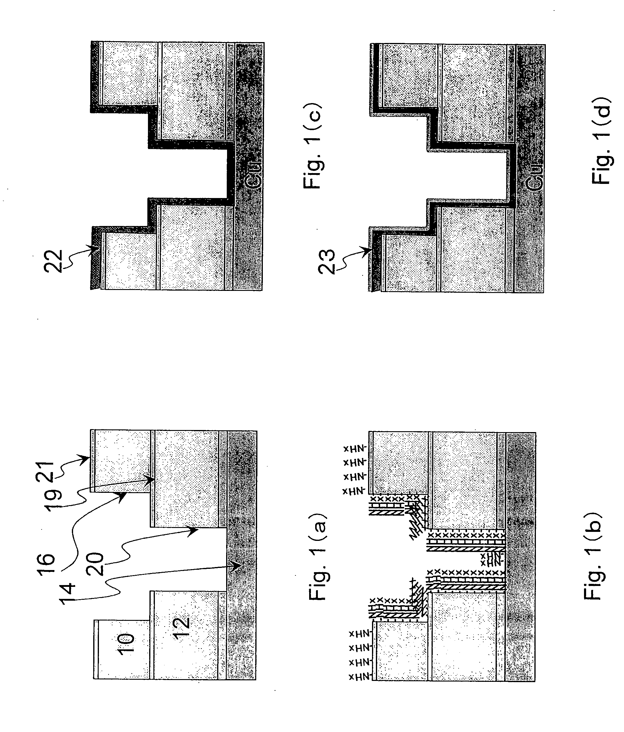
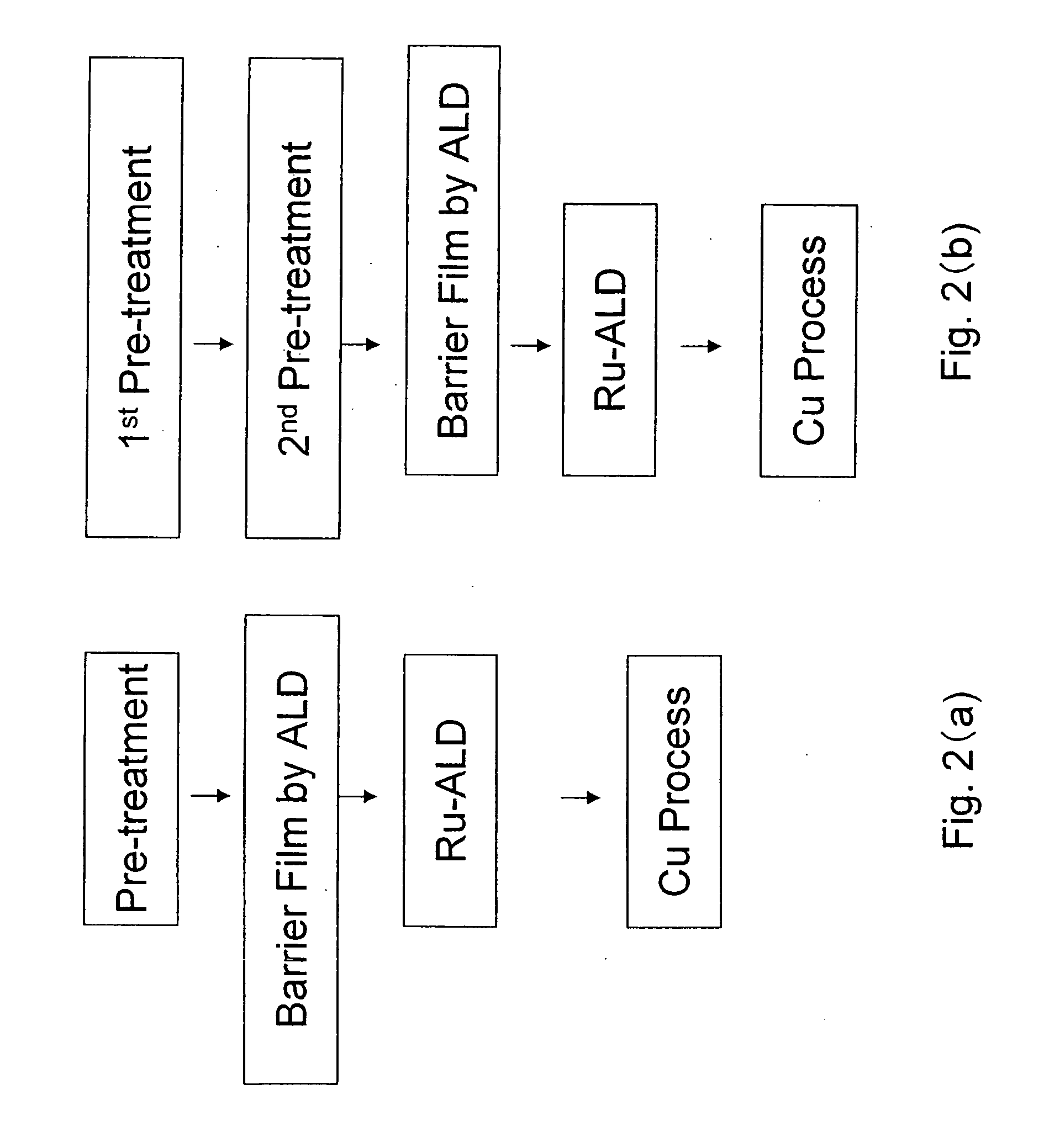
[0216] This example illustrates a process of lining with a metal film, which becomes a copper barrier film, the entire surface of trenches and contact vias of a dual damascene structure to create a semiconductor element. Specifically, the process relates to the step to pre-treat the entire surface of trenches (16) and contact vias (20) of the dual damascene structure, the step to form a tungsten carbon nitride WNC film as a metal barrier film, and the step to form a Ru film, corresponding to FIGS. 1(b), (c) and (d), respectively. These steps correspond to the flow shown in FIG. 5(a) or (b), and the steps corresponding to FIGS. 1(b), (c) and (d) are implemented using an apparatus having the structure shown in FIG. 5(c). A semiconductor substrate on which the structure shown in the schematic cross-section drawing per FIG. 1(a) was transferred from the cassette box (100) to the load lock chamber (102) by means of the atmospheric pressure robot (101), as shown in FIG. 5(c). After the ch...

example 1-1

[0226] FIGS. 8(a) and (b) show cross-section images of a trench structure where a WNC-ALD film was formed, after pre-treatment, on a SiOC film (201) formed by plasma CVD (Aurora ULKTM film by ASM). Pre-treatment 2 shown in Tables 3 and 4 was implemented, after which a WNC film was formed using the WNC-ALD formation method explained above. FIG. 8(a) shows an extremely uniform, smooth WNC film (202) formed at a RF power of 100 W. FIG. 8(b) shows a similarly uniform, smooth WNC film (203) formed at a RF power of 300 W.

example 1-2

[0227]FIG. 9(a) and (b) show film conditions on a plasma CVD film (201) (Aurora ULKTM film by ASM), when the conditions of pre-treatments 1 and 2 shown in Table 3 were implemented separately. FIG. 9(a) shows the condition after pre-treatment 1 in which plasma process using H2 / He mixture gas was performed. As shown by the TEM cross-section image of the trench, the WNC-ALD film (204) is neither continuous nor smooth on the side face. The purpose of pre-treatment 1 is to reduce copper oxide film, and this image shows that this pre-treatment alone is not always effective in introducing amino groups to the surface of low dielectric constant film. On the other hand, FIG. 9(b) shows the condition after performing pre-treatment 2 using H2 / H2 / N2 mixture gas. As shown, the WNC-ALD film (205) is continuous and smooth even on the side face of the trench. Since there is not need to reduce copper oxide film here, pre-treatment 1 can be omitted. The same shape was also obtained under the pre-treat...


PUM

PropertyMeasurementUnit
Temperatureaaaaaaaaaa
Shrinkageaaaaaaaaaa

Abstract

A method for forming a metal wiring structure includes: (i) providing a multi-layer structure including an exposed wiring layer and an exposed insulating layer in a reaction space; (ii) introducing an —NH2 or >NH terminal at least on an exposed surface of the insulating layer in a reducing atmosphere; (iii) introducing a reducing compound to the reaction space and then purging a reaction space; (iv) introducing a metal halide compound to the reaction space and then purging the reaction space; (v) introducing a gas containing N and H and then purging the reaction space; (vi) repeating steps (iii) to (v) in sequence to produce a metal-containing barrier layer; and (vii) forming a metal film on the metal-containing barrier layer.

Description

CROSS REFERENCE TO RELATED APPLICATIONS [0001] This is a continuation-in-part of U.S. patent application Ser. No. 11 / 245,908, field Oct. 7, 2005, the disclosure of which is herein incorporated by reference in its entirety.BACKGROUND OF THE INVENTION [0002] 1. Field of the Invention [0003] The present invention relates to a method for forming metal wiring structures that can be used favorably in producing fine semiconductor devices. [0004] 2. Description of the Related Art [0005] In the formation of wiring layers in semiconductor devices, insulation films of low dielectric constant are used as insulation layers between wires, while Cu and other metal wires of low resistance are used for wires, in order to prevent delays in signal transmission. When forming a Cu wiring structure, a general method is to form an interlayer insulation film on the Cu wiring in the bottom layer, and then form in this insulation film a lower layer and trenches that become a wiring pattern in an upper layer ...

Claims


Application Information

Patent Timeline
IPC IPC(8): C23C16/00
CPCC23C16/0245C23C16/18C23C16/36C23C16/45529C23C16/45542H01L21/02063H01L21/28556H01L21/3105H01L21/76807H01L21/76814H01L21/76843H01L21/76846H01L21/28562H01L21/76826H01L21/76831H01L23/53238H01L23/53295H01L28/90H01L21/28H01L21/3205
Inventor SHINRIKI, HIROSHISHIMIZU, AKIRA
Owner ASM JAPAN
Why Eureka
Try Eureka