High-heat-resistant semiconductor device
- Summary
- Abstract
- Description
- Claims
- Application Information
AI Technical Summary
Benefits of technology
Problems solved by technology
Method used
Image

Examples
first example
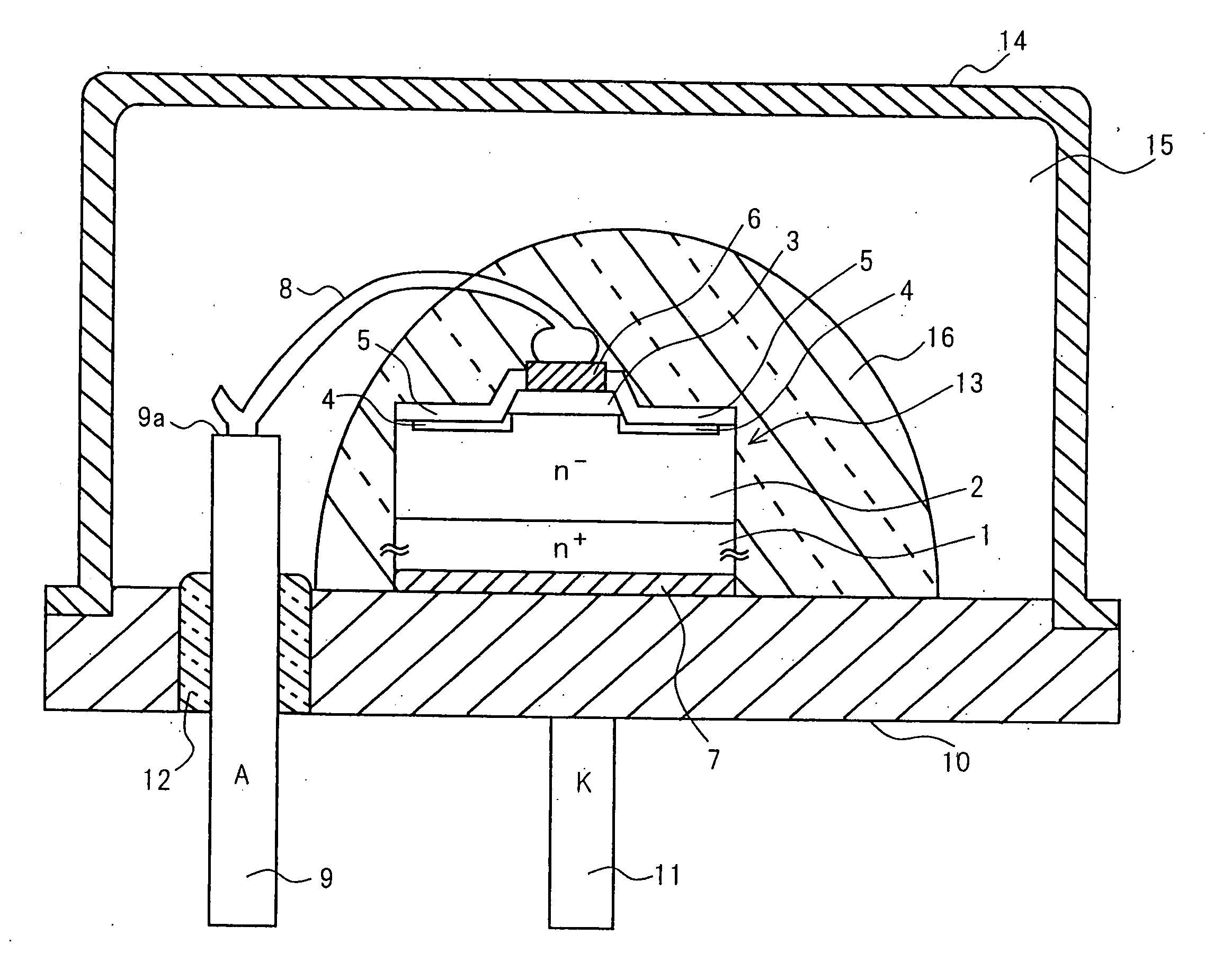
[0078] A high-heat-resistant semiconductor device according to a first example of the present invention will be described with reference to FIG. 1.
[0079] The semiconductor device according to the first example of the invention is a SiC (silicon carbide) pn diode high in heat resistance and withstand voltage.
[0080]FIG. 1 is a cross-sectional view of the SiC pn diode with a withstand voltage of 8 kV according to the first example of the invention. In FIG. 1, a SiC diode element 13 has the following structure. An about 90 μm thick n-type SiC drift layer 2 with a low impurity concentration is formed on the upper surface of an about 300 μm thick n-type SiC cathode region 1 with a high impurity concentration. A cathode electrode 7 is formed on the lower surface of the cathode region 1. A p-type SiC anode region 3 forming a main junction is formed on the central region of the drift layer 2.
[0081] A metal anode electrode 6 is formed on the anode region 3. A p-type field-relief region 4 i...
second example
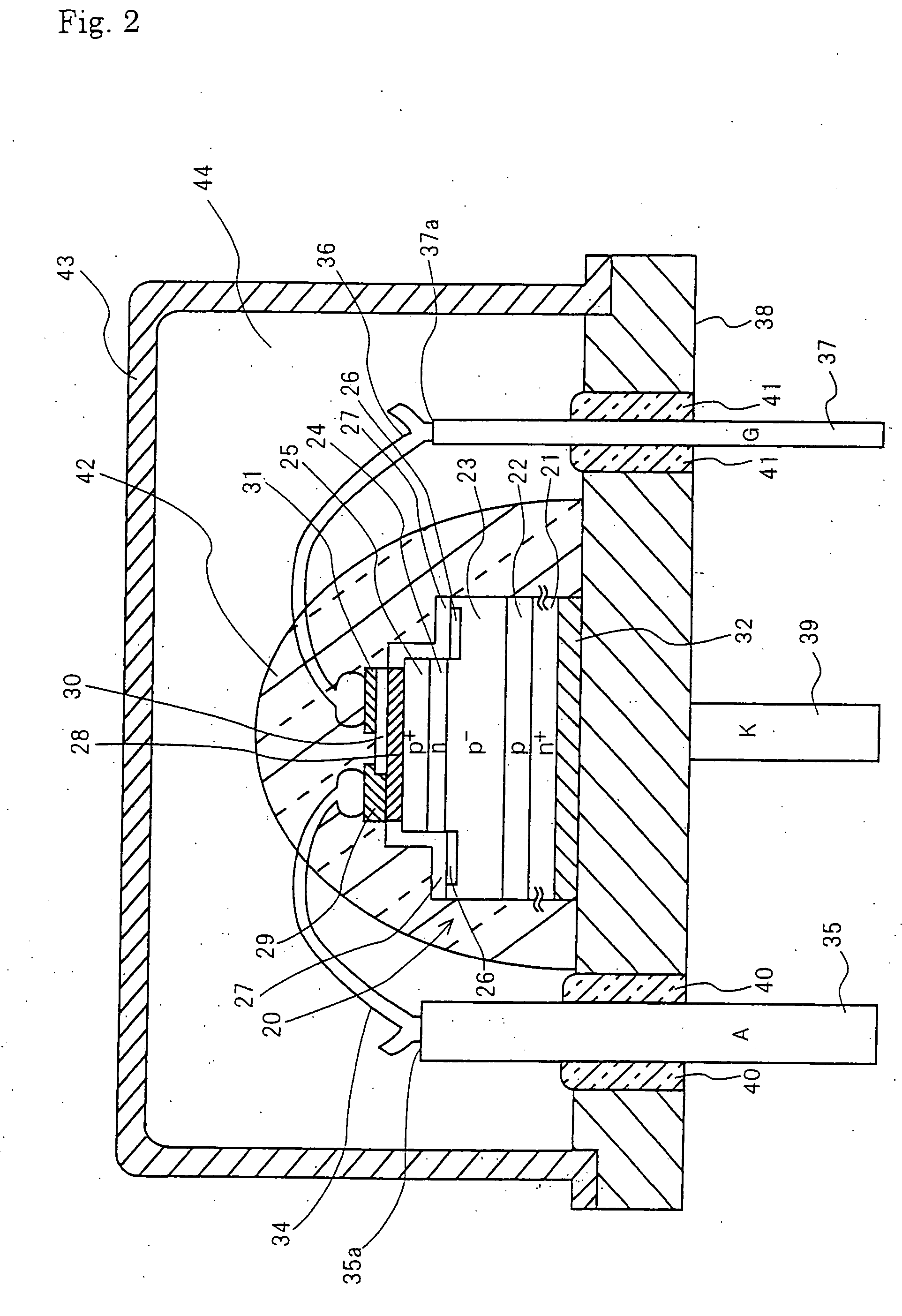
[0090] A semiconductor device according to a second example of the invention is a SiC-GTO thyristor (gate turn off thyristor) device having a withstand voltage of 5 kV, and FIG. 2 is a cross-sectional view of the thyristor. FIG. 3 is a cross-sectional view of a cell indicated by cutting the GTO thyristor element 20 along a direction which is vertical to a sheet of paper in which FIG. 2 is represented. With the actual element, the cell shown in FIG. 3 is present plurally, that is, the cells are linked along the lateral direction of FIG. 3. In FIGS. 2 and 3, a p-type SiC buffer layer 22 about 3 μm thick is provided on the upper surface of a n-type SiC cathode region 21 about 320 μm thick having a high impurity concentration. A cathode electrode 32 is provided on the lower surface of the cathode region 21. A p-type SiC drift layer 23 abort 60 μm thick having a low impurity concentration is provided on the buffer layer 22. A n-type base region 24 about 2 μm thick and a p-type anode regi...
third example
[0104] A semiconductor device according to a third example of the invention is a photocoupled wide gap power semiconductor device and FIG. 4 is a cross-sectional view of the semiconductor device. In FIG. 4, a GaN (gallium nitride)-npn bipolar transistor 51 having a withstand voltage of 3 kV and a current capacity of 200 A is used as a main power semiconductor element having a light emitting function. As a light receiving element, a SiC photodiode 52 is used. The SiC photodiode 52 and the GaN-npn bipolar transistor 51 are provided oppositely each other within a package.
[0105] In the GaN-npn bipolar transistor 51 shown in FIG. 4, a p-type GaN base region 54 about 1.7 μm thick and a n-type emitter region 55 about 3μm thick having a high impurity concentration are formed on the upper surface of a n-type GaN collector region 53 about 300 μm thick having a high impurity concentration in that order. A collector electrode 66 is provided on the lower surface of the GaN collector region 53. ...
PUM
| Property | Measurement | Unit |
|---|---|---|
| Time | aaaaa | aaaaa |
| Structure | aaaaa | aaaaa |
| Molecular weight | aaaaa | aaaaa |
Abstract
Description
Claims
Application Information