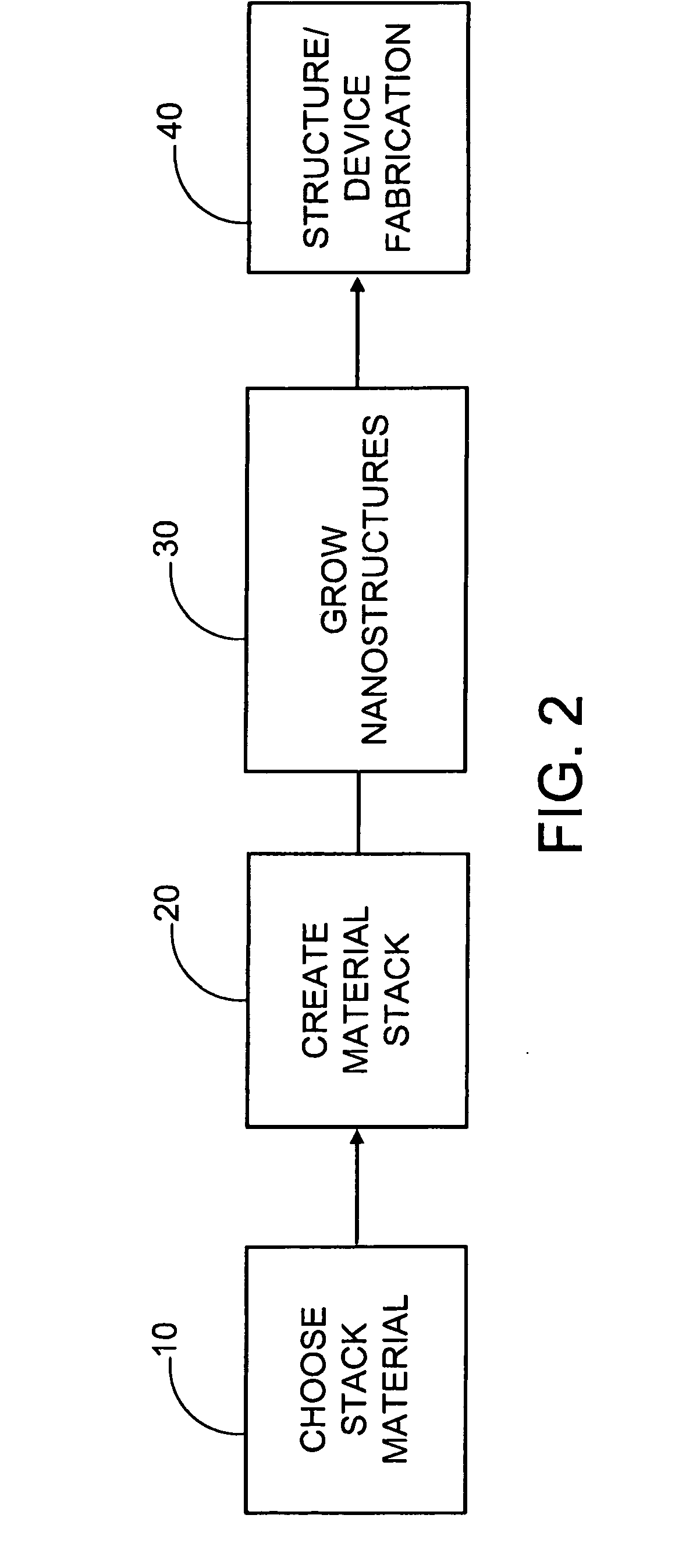
Interconnects and heat dissipators based on nanostructures
a technology of interconnections and heat dissipators, applied in the field of nanostructures, can solve the problems of inability to achieve perfect control, increase the cost of new materials, and increase the cost of traditional materials used in making devices
- Summary
- Abstract
- Description
- Claims
- Application Information
AI Technical Summary
Problems solved by technology
Method used
Image

Examples
example 1
Control
[0154] This example presents results that evidence control over the morphology and control over the chemical composition present at the base and the tip of grown carbon nanostructures, see FIGS. 17A and 17B. FIG. 17A is a transmission electron microscopy (TEM) micrograph showing a carbon nanofiber grown on a W metal underlayer. FIG. 17A shows how the morphology can differ based on sample preparation recipe.
[0155]FIG. 17B shows an example of how the chemical composition at the interface (base) and at the tip can be obtained. In FIG. 17B panel (a) there is a TEM image of a grown carbon nanofiber; in panel (b) an EDS spectrum shows the chemical elements at the tip of the fibers (catalyst region); and in panel (c) an EDS spectrum shows the chemical elements at the base of the fibers (underlayer region).
[0156] The CNF grew from a flat catalyst surface and no significant catalyst film break up was observed (see, e.g., Kabir, M. S.; Morjan, R. E.; Nerushev, O. A.; Lundgren, P.; B...
example 2
Incorporating Nanostructures into a CMOS Device
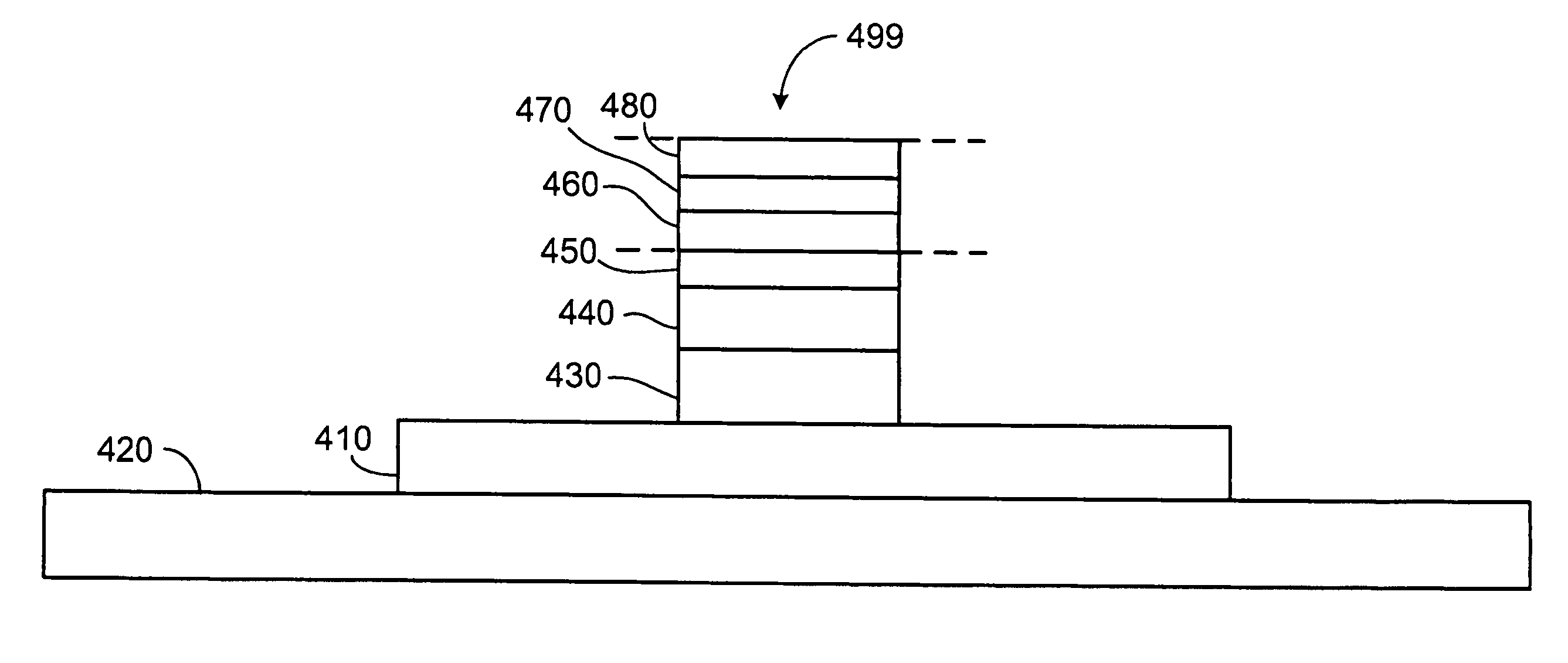
[0157] Nanostructures as described herein can be incorporated into a CMOS device as vertical interconnects. To accomplish this, a filler layer such as an insulator is deposited over a substrate and the nanostructures situated thereon, and then polished / etched back until the nanostructure is exposed at the top. The catalyst layer can be removed, e.g., by etching, once the nanostructure is grown if required.
example 3
Lift-Off Method for Growing Localized Nanostructures
[0158] The present invention also encompasses a method of making nanostructures that are localized at specific positions, rather than being formed in arrays from a continuous film on a substrate. This method obviates the requirement of other processes in the art to anneal a film of catalyst to create discrete particles of catalyst in an uncontrolled manner.
[0159] According to this method, a metal layer, e.g., on a silicon substrate, is coated with a polymer layer. Such a polymer layer may be a photo-sensitive layer. The polymer layer is patterned by one of the several methods known in the art to define regions where one or more nanostructures are desired. The regions of polymer so patterned, i.e., where the nanostructures are intended to be positioned, are then removed, thus forming cavities in the polymer layer. A layer of insulator, e.g., amorphous silicon, is deposited over the polymer, followed by another layer of catalyst. T...
PUM
| Property | Measurement | Unit |
|---|---|---|
| thick | aaaaa | aaaaa |
| thick | aaaaa | aaaaa |
| temperatures | aaaaa | aaaaa |
Abstract
Description
Claims
Application Information
 - R&D
- Intellectual Property
- Life Sciences
- Materials
- Tech Scout
- Unparalleled Data Quality
- Higher Quality Content
- 60% Fewer Hallucinations
Browse by: Latest US Patents, China's latest patents, Technical Efficacy Thesaurus, Application Domain, Technology Topic, Popular Technical Reports.
© 2025 PatSnap. All rights reserved.Legal|Privacy policy|Modern Slavery Act Transparency Statement|Sitemap|About US| Contact US: help@patsnap.com