
Semiconductor integrated circuit device and method for fabricating the same

Active Publication Date: 2007-05-24
PANASONIC CORP
View PDF9 Cites 7 Cited by
  • Summary
  • Abstract
  • Description
  • Claims
  • Application Information

AI Technical Summary

Benefits of technology

[0012] It is therefore an object of the present invention to provide a semiconductor integrated circuit device in which a microstrip line is easily formed and a field effect transistor exhibiting excellent heat dissipation is included.
[0013] To achieve the object, according to the present invention, a semiconductor integrated circuit device has a structure in which a substrate for crystal growth is separated from a semiconductor layer and interconnections on the upper and lower faces of the semiconductor from which the substrate has been removed form a microstrip line. In this manner, a microstrip line is easily formed, thereby achieving size reduction of a chip. In addition, separation of the crystal growth substrate enables enhancement of heat dissipation.
[0014] Specifically, a through hole for exposing one of a source electrode, a drain electrode and a gate electrode is formed in a semiconductor layer and an insulating film formed on the semiconductor layer. Interconnections electrically connected to the electrodes through the through holes are provided to face each other with the semiconductor layer and the insulating film sandwiched therebetween, thereby forming a microstrip line. This microstrip line is combined as a passive element with at least one field effect transistor (FET), thereby forming a semiconductor integrated circuit device. In addition, since the semiconductor layer has been separated from a crystal growth substrate, so that it is unnecessary to provide a through hole for forming interconnection in the crystal growth substrate, and only providing a through hole in the semiconductor layer and the insulating film allows a microstrip line to be formed. Accordingly, an RF integrated circuit device with a small chip area is easily formed. Moreover, if a supporting substrate exhibiting excellent heat dissipation is bonded to the semiconductor layer from which the crystal growth substrate has been removed, a semiconductor integrated circuit device exhibiting excellent heat dissipation is implemented.

Problems solved by technology

In the case of using a sapphire substrate widely used for crystal growth of nitride semiconductor, it generally difficult to process the sapphire substrate by dry etching, so that a through hole, i.e., a via hole, cannot be formed.
In each of the conventional semiconductor integrated circuit devices including GaN-based FETs described above, however, the coplanar line is used and the ground line is formed on the surface of a chip, so that the problem of limitation on reduction of the chip area arises.
Accordingly, another problem in which the fabrication process becomes complicated arises.
Furthermore, since sapphire is used for a substrate for the growth of a nitride semiconductor layer, heat dissipation is not good and enhancement of electrical characteristics during high-power operation is limited.

Method used


Image

  • Semiconductor integrated circuit device and method for fabricating the same
  • Semiconductor integrated circuit device and method for fabricating the same
  • Semiconductor integrated circuit device and method for fabricating the same

Examples


embodiment 1

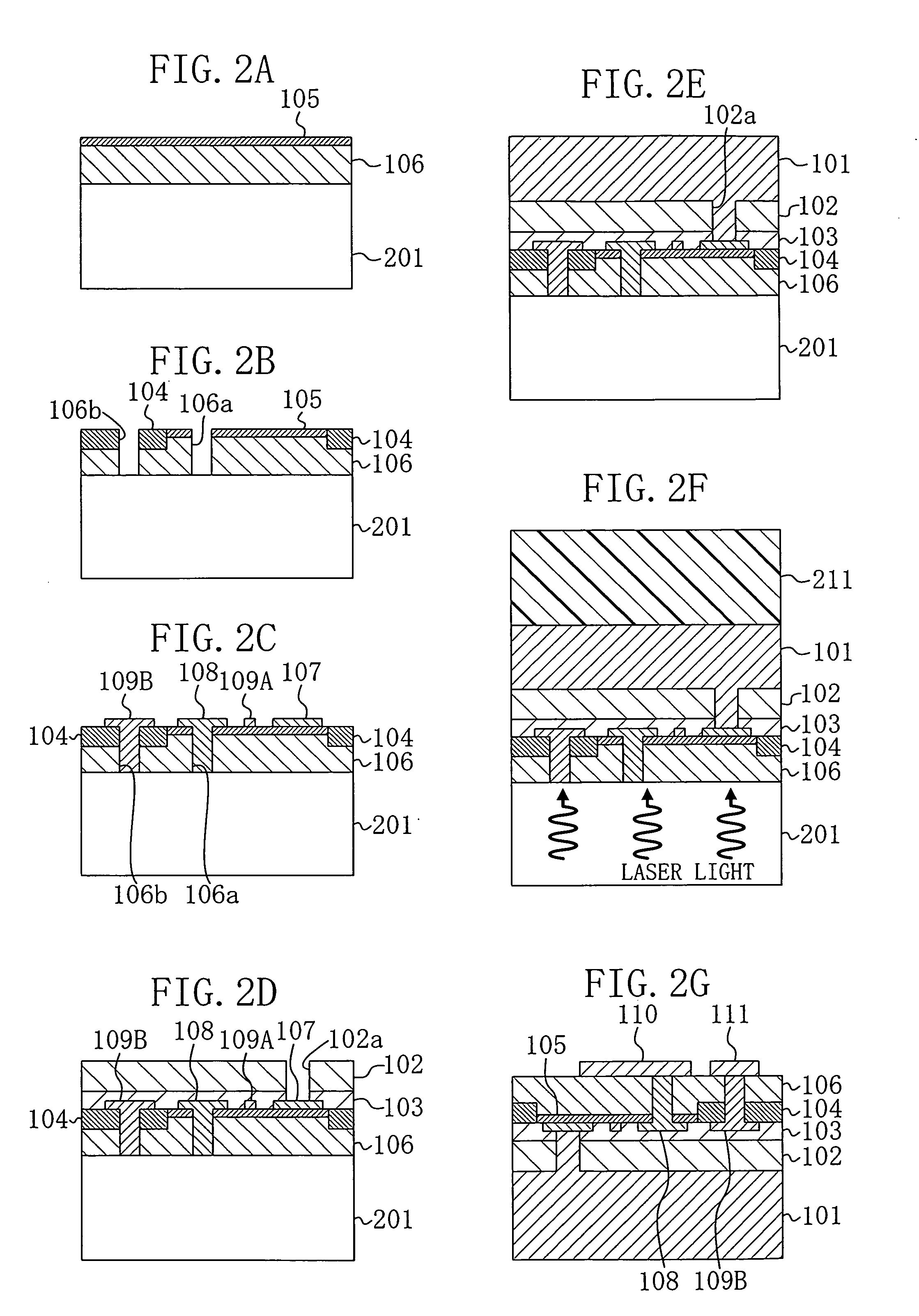
[0044] A first embodiment of the present invention will be described with reference to the drawings.

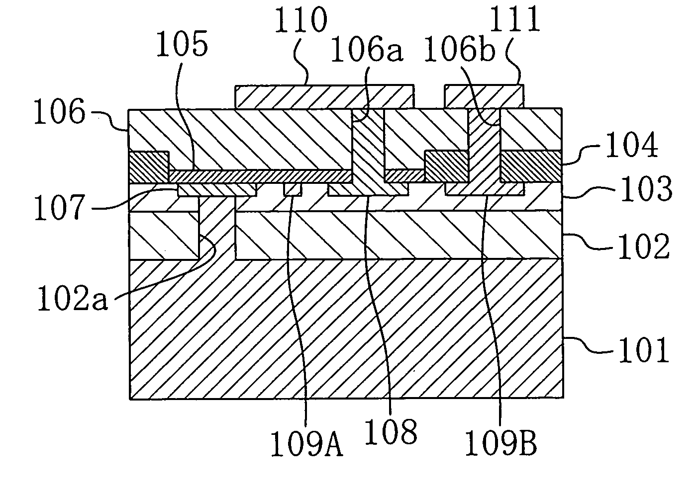
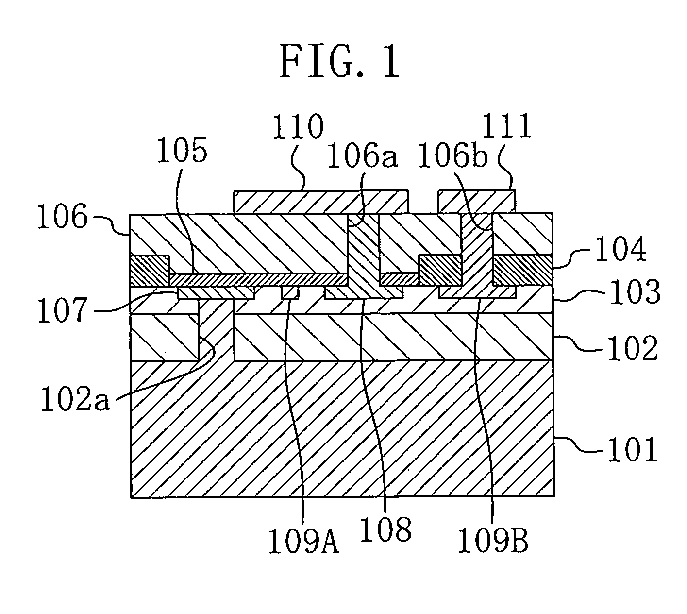
[0045]FIG. 1 is a cross-sectional view of a semiconductor integrated circuit device according to a first embodiment of the present invention. As illustrated in FIG. 1, an interlayer insulating film 102 made of benzo-cyclo-butene (BCB) with a thickness of about 3 μm, a passivation film 103 made of silicon nitride (SiN), a first semiconductor layer 105 made of n-type AlGaN and a second semiconductor layer 106 made of undoped GaN are sequentially formed on, for example, a source line 101 made of gold (Au) plating with a thickness of 10 μm or more.

[0046] A gate electrode 109A and source and drain electrodes 107 and 108 formed at both sides of the gate electrode 109A with spacing are formed on the lower face of the first semiconductor layer 105.

[0047] A first through hole 102a in which the source electrode 107 is exposed is formed in the interlayer insulating film 102 and the passivatio...

embodiment 2

[0066] Hereinafter, a second embodiment of the present invention will be described with reference to the drawings.

[0067]FIG. 3 illustrates a cross-sectional structure of a semiconductor integrated circuit device according to the second embodiment. As illustrated in FIG. 3, a passivation film 303 made of silicon nitride (SiN) is bonded to a supporting substrate 301 made of, for example, semi-insulating silicon carbide (SiC) with a thickness of 150 μm or more with an electrode pattern 302 of gold (Au) / gold tin (AuSn) / gold (Au), a drain line 312 and a gate line 313 sandwiched therebetween.

[0068] A first semiconductor layer 304 made of n-type AlGaN, a second semiconductor layer 305 made of undoped GaN, a buffer layer 306 made of AlN, an interlayer insulating film 314 made of benzo-cyclo-butene (BCB) with a thickness of about 3 μm and a source line 311 are sequentially formed on the passivation film 303.

[0069] A gate electrode 309A is formed on the lower face of the first semiconducto...

embodiment 3

[0089] Hereinafter, a third embodiment of the present invention will be described with reference to the drawings.

[0090]FIG. 5 illustrates a cross-sectional structure of a semiconductor integrated circuit device according to the third embodiment. As illustrated in FIG. 5, a first semiconductor layer 502 made of undoped GaN and a second semiconductor layer 503 made of n-type AlGaN are attached to a supporting substrate 501 having a thickness of, for example, 150 μm or more and made of silicon (Si) whose principal surface has a plane orientation of a (100) plane with an electrode pattern 510 made of Au / AuSn / Au and a source line 509 sandwiched therebetween.

[0091] A gate electrode 506A is formed on the second semiconductor layer 503 and a source electrode 504 and a drain electrode 505 are formed at both sides of the gate electrode 506A with spacing on the second semiconductor layer 503.

[0092] A high-resistance region 507 formed to have a high resistance by, for example, selective oxid...


PUM


Abstract

A semiconductor integrated circuit device includes: a semiconductor layer having a principal surface on which a source electrode, a drain electrode and a gate electrode are formed and having a first through hole; an insulating film formed in contact with the semiconductor layer and having a second through hole; a first interconnection formed on the semiconductor layer through the first through hole and connected to one of the source electrode, the drain electrode and the gate electrode which is exposed in the first through hole; and a second interconnection formed on the insulating film through the second through hole and connected to another of the source electrode, the drain electrode and the gate electrode which is exposed in the second through hole. The first interconnection and the second interconnection face each other and form a microstrip line.

Description

CROSS-REFERENCE TO RELATED APPLICATION [0001] The disclosure of Japanese Patent Application No. 2005-333860 filed in Japan on Nov. 18, 2005 including specification, drawings and claims is incorporated herein by reference in its entirety. BACKGROUND OF THE INVENTION [0002] The present invention relates to semiconductor integrated circuit devices including field effect transistors (FETs) using nitride semiconductor applicable to radio frequency (RF) transistors and methods for fabricating the devices. [0003] Compound semiconductor of a Group-III nitride typified by gallium nitride (GaN) is wide-gap semiconductor having a large band gap and has characteristics of a dielectric strength higher than that of, for example, compound semiconductor such as gallium arsenide (GaAs) or semiconductor such as silicon (Si) and a high saturation drift speed of electrons. Accordingly, compound semiconductor has attracted attention for use in RF high-power transistors and has been intensively studied a...

Claims


Application Information

Patent Timeline
IPC IPC(8): H01L29/94
CPCH01L21/6835H01L21/76898H01L23/66H01L2221/6835H01L2223/6627H01L2924/14H01L2924/19032H01L2924/19041H01L2924/19042H01L2924/30105H01L2924/0002H01L2924/00H01L29/4175H01L29/2003H01L29/7787
Inventor UEDA, TETSUZOTANAKA, TSUYOSHI
Owner PANASONIC CORP
Features
  • Generate Ideas
  • Intellectual Property
  • Life Sciences
  • Materials
  • Tech Scout
  • Unparalleled Data Quality
  • Higher Quality Content
  • 60% Fewer Hallucinations
Learn More