Semiconductor device and method of manufacturing the same

a semiconductor and semiconductor technology, applied in the field of semiconductor devices, can solve the problems of difficult manufacturing of tft having satisfactory performance to meet the circuit specification, unsuitable to use amorphous semiconductor films, etc., and achieve the effects of reducing the surface energy, enhancing the diffusion of semiconductor atoms, and reducing the cost of production

Inactive Publication Date: 2007-05-24
SEMICON ENERGY LAB CO LTD
View PDF73 Cites 8 Cited by
  • Summary
  • Abstract
  • Description
  • Claims
  • Application Information

AI Technical Summary

Benefits of technology

[0027] This step first has an effect to flatten the surface of the crystal-containing semiconductor film. This is a result of enhanced surface diffusion of semiconductor atoms functioning to make the surface energy minimum. Besides, at the same time, this step has also an effect to greatly decrease defects existing in crystal grains and crystal grain boundaries. This effect is obtained through a terminating effect to uncombined bonds by hydrogen, a removing effect to impurities by hydrogen, and recombination of semiconductor atoms with the effect. For the purpose of obtaining these effects, the heat treatment at 900 to 1200° C. in the reduced atmosphere is necessary.
[0035] This third step has an effect to further flatten the surface of the crystal-containing semiconductor film. This is a result of enhanced surface diffusion of semiconductor atoms functioning to make the surface energy minimum. Besides, at the same time, this step has also an effect to greatly decrease defects existing in crystal grains and crystal grain boundaries. This effect is obtained through a terminating effect to uncombined bonds by hydrogen, a removing effect to impurities by hydrogen, and recombination of semiconductor atoms with the effect. For the purpose of obtaining these effects, the heat treatment at 900 to 1200° C. in the reduced atmosphere is necessary.
[0036] In the fourth step, the step of oxidizing the film to decrease its thickness may be carried out through a plurality of thermal oxidation steps. As means for oxidizing the film to decrease its thickness, it is possible to use thermal oxidation, plasma oxidation, or the like. Particularly, in the present invention, oxidation through the thermal oxidation is preferable. Incidentally, in the case of the plasma oxidation, if He is added in an oxygen atmosphere, an oxygen radical is easily produced. Thus, the addition of He is preferable. Besides, in the fourth step, it is possible to obtain an effect to flatten the roughness of the surface of the semiconductor film.
[0052] In the third step, the step of oxidizing the film to decrease its thickness may be carried out through a plurality of thermal oxidation steps. As means for oxidizing the film to decrease its thickness, it is possible to use thermal oxidation, plasma oxidation, or the like. Particularly, in the present invention, oxidation through the thermal oxidation is preferable. In the case of the plasma oxidation, if He is added in an oxygen atmosphere, an oxygen radical is easily produced. Thus, the addition of He is preferable. Besides, in the third step, it is possible to obtain an effect to flatten the roughness of the surface of the semiconductor film.
[0054] This fourth step has an effect to further flatten the surface of the crystal-containing semiconductor film. This is a result of enhanced surface diffusion of semiconductor atoms functioning to make the surface energy minimum. Besides, at the same time, this step has also an effect to greatly decrease defects existing in crystal grains and crystal grain boundaries. This effect is obtained through a terminating effect to uncombined bonds by hydrogen, a removing effect to impurities by hydrogen, and recombination of semiconductor atoms with the effect. For the purpose of obtaining these effects, the heat treatment at 900 to 1200° C. in the reduced atmosphere is necessary.

Problems solved by technology

Since such a driver circuit or a logic circuit is required to perform a high speed operation, it is unsuitable to use an amorphous semiconductor film (typically, an amorphous silicon film) as an active layer.
However, when circuit performance comparable to a conventional IC comes to be required for a circuit assembled with TFTs, such circumstances have occurred that it is difficult to manufacture a TFT having satisfactory performance to meet the circuit specification by using a crystalline semiconductor film formed through a conventional technique.

Method used


Image

  • Semiconductor device and method of manufacturing the same
  • Semiconductor device and method of manufacturing the same
  • Semiconductor device and method of manufacturing the same

Examples


embodiment 1

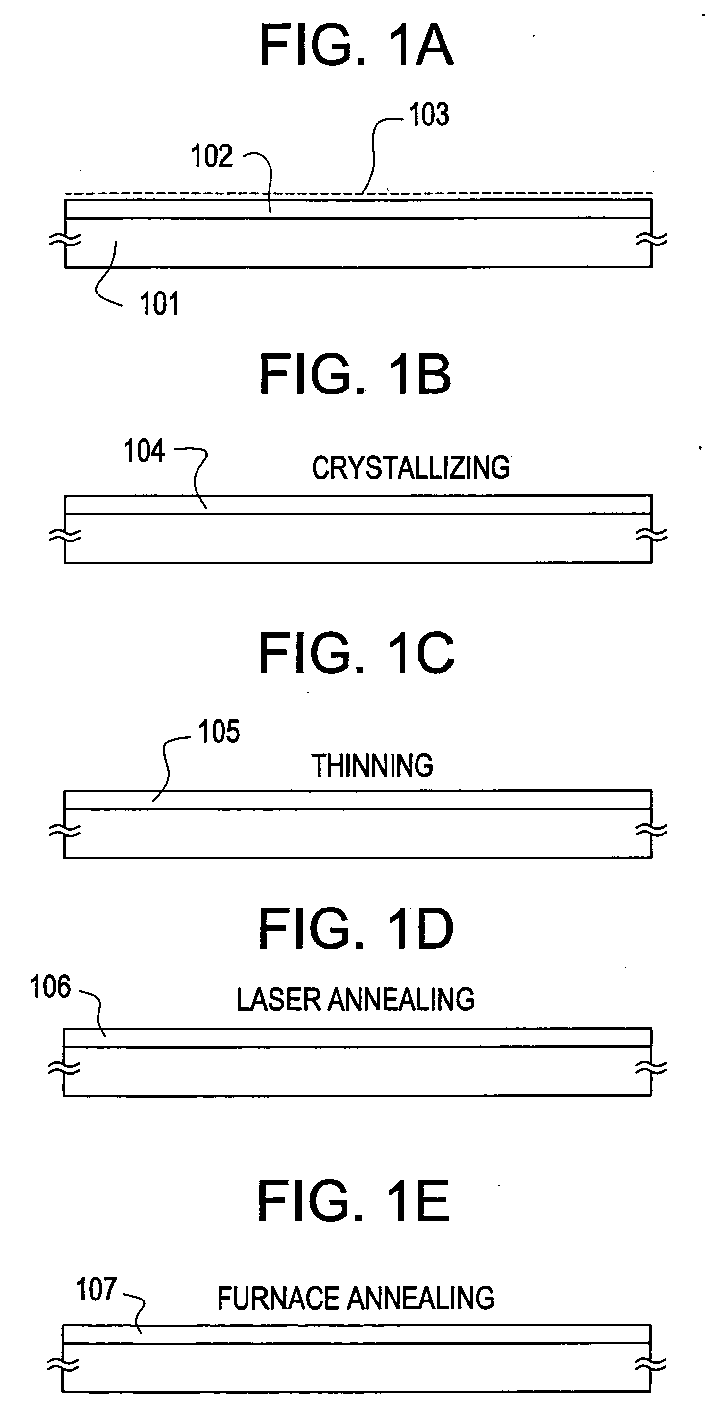
[0080] In this embodiment, steps of manufacturing a TFT over a substrate by carrying out the present invention will be described. FIGS. 1A to 1E will be used for the description.

[0081] First, a quartz substrate 101 was prepared. A material having high heat resistance must be selected as the substrate. Instead of the quartz substrate, a substrate of a material having high heat resistance, such as a silicon substrate, a ceramic substrate, a crystallized glass substrate, or a metal substrate may be used.

[0082] However, although an underlying film may not be provided in the case where the quartz substrate is used, it is preferable to provide an insulating film as the underlying film in the case where other materials are used. As the insulating film, it is appropriate that either one of a silicon oxide film (SiOx), a silicon nitride film (SixNy), a silicon oxynitride film (SiOxNy), and an aluminum nitride film (AlxNy), or a laminated film of those is used.

[0083] Besides, it is effecti...

embodiment 2

[0137] In this embodiment, an example in which an initial film first formed on a substrate is made a polysilicon film, will be described with reference to FIGS. 3A to 3D.

[0138] First, an underlying film 302 made of a silicon oxide film, a polysilicon film 303 with a thickness of 75 nm, and a protection film 304 are continuously formed and laminated on a metal substrate (in this embodiment, tantalum substrate) 301 without making opening to the air. Incidentally, in this embodiment, film formation is carried out in a multichamber system low pressure CVD apparatus having a vacuum load-lock chamber and a common chamber. (FIG. 3A)

[0139] Next, a thermal oxidation step at 1050° C. for 30 minutes is carried out. In this embodiment, for the purpose of carrying out the heat treatment while relieving stress, a wet oxidation method containing water vapor was used. The thickness of a polysilicon film 305 obtained through this step is decreased through the oxidation to 50 nm. The thickness of t...

embodiment 3

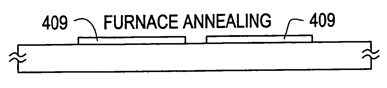
[0148] In this embodiment, an example in which crystallization of an amorphous silicon film as an initial film is carried out by a technique disclosed in Japanese Patent Application Laid-open No. 8-78329, will be described with reference to FIGS. 4A to 4G. An entire disclosure of the Japanese Patent Application No. 8-78329 is incorporated herein by reference.

[0149] First, a quartz substrate 401 having a surface provided with an insulating film is prepared, and an amorphous silicon film (not shown) and a silicon oxide film (not shown) are continuously formed and laminated thereon without making opening to the air. Next, the silicon oxide film is patterned to form a mask 402 having an opening portion.

[0150] Next, a solution containing nickel of 100 ppm in terms of weight is applied by a spin coating method, so that such a state that the amorphous silicon film is in contact with nickel is obtained at the bottom of the opening portion. Thereafter, a furnace annealing step at 570° C. f...


PUM

PropertyMeasurementUnit
wavelengthaaaaaaaaaa

Abstract

There is provided a method in which a TFT with superior electrical characteristics is manufactured and a high performance semiconductor device is realized by assembling a circuit with the TFT. The method of manufacturing the semiconductor device includes: a step of forming a crystal-containing semiconductor film by carrying out a thermal annealing to a semiconductor film; a step of carrying out an oxidizing treatment to the crystal-containing semiconductor film; a step of carrying out a laser annealing treatment to the crystal-containing semiconductor film after the oxidizing treatment has been carried out; and a step of carrying out a furnace annealing treatment to the crystal-containing semiconductor film after the laser annealing. The laser annealing treatment is carried out with an energy density of 250 to 5000 mJ / cm2.

Description

BACKGROUND OF THE INVENTION [0001] 1. Field of the Invention [0002] The present invention relates to a semiconductor device which includes, as a circuit, a thin film transistor (hereinafter referred to as TFT) using a semiconductor thin film, and a technique regarding a method of manufacturing the same. Incidentally, in the present specification, the semiconductor device means any device which is made to function by using a semiconductor. [0003] Thus, the term “semiconductor device” recited throughout this specification includes not only a single semiconductor component such as a TFT, but also an electro-optical device with TFTs, a semiconductor circuit, and an electronic equipment having those. [0004] 2. Description of the Related Art [0005] In recent years, a TFT used for an electro-optical device such as an active matrix type liquid crystal display device has been actively developed. The active matrix type liquid crystal display device is a monolithic display device in which a pi...

Claims


Application Information

Patent Timeline
Patent Type & Authority Applications(United States)
IPC IPC(8): H01L21/84H01L31/113G02F1/1362H01L21/20H01L21/268H01L21/336H01L29/786
CPCG02F1/13454H01L21/2022H01L21/2026H01L21/268H01L27/1285H01L29/66757H01L29/78675H01L27/1277H01L29/04H01L21/02686H01L21/02672H01L21/0262H01L21/02532
Inventor OHTANI, HISASHITAKANO, TAMAEYAMAZAKI, SHUNPEI
Owner SEMICON ENERGY LAB CO LTD
Why Eureka
Try Eureka