Chemical mechanical polishing method and method of manufacturing semiconductor device

a technology of mechanical polishing and semiconductor devices, which is applied in the direction of manufacturing tools, lapping machines, other chemical processes, etc., can solve the problem of not being able to achieve the flatness of the first organic film b>9/b>, and achieve the effect of reducing the resistance of metal interconnects and wire-to-wire capacitance, reducing the number of steps, and increasing yield

Inactive Publication Date: 2007-06-07
JSR CORPORATIOON +1
View PDF8 Cites 29 Cited by
  • Summary
  • Abstract
  • Description
  • Claims
  • Application Information

AI Technical Summary

Benefits of technology

[0103] The effects of the chemical mechanical polishing method according to this embodiment are described below. First, related-art organic film polishing is described for comparison.
[0104] In recent years, a damascene interconnect has been mainly utilized to reduce the resistance of the metal interconnect and the wire-to-wire capacitance in a semiconductor integrated circuit device.
[0105] A “dual damascene structure” which is formed by collectively processing an interconnect groove and a contact (via) has been employed for the damascene interconnect from the viewpoint of reducing the number of steps and increasing the yield. As the dual damascene structure, a hybrid structure in which two different low-dielectric-constant films are used for the interconnect and the via has been employed from the viewpoint of controllability of the pro...

Problems solved by technology

As a result, the flatness of the first organic film 9 cannot be achieved...

Method used


Image

  • Chemical mechanical polishing method and method of manufacturing semiconductor device
  • Chemical mechanical polishing method and method of manufacturing semiconductor device
  • Chemical mechanical polishing method and method of manufacturing semiconductor device

Examples


example 1

2-1. Example 1

[0133] This example illustrates a hybrid dual damascene processing method by a dual hard mask method using an ArF excimer laser incorporating planarization of an organic film by CMP.

[0134] This example illustrates the case of chemical mechanical polishing the first organic film 9 using the above slurry 1.

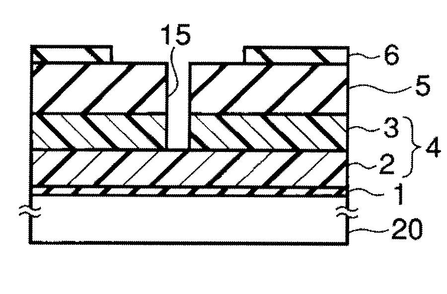
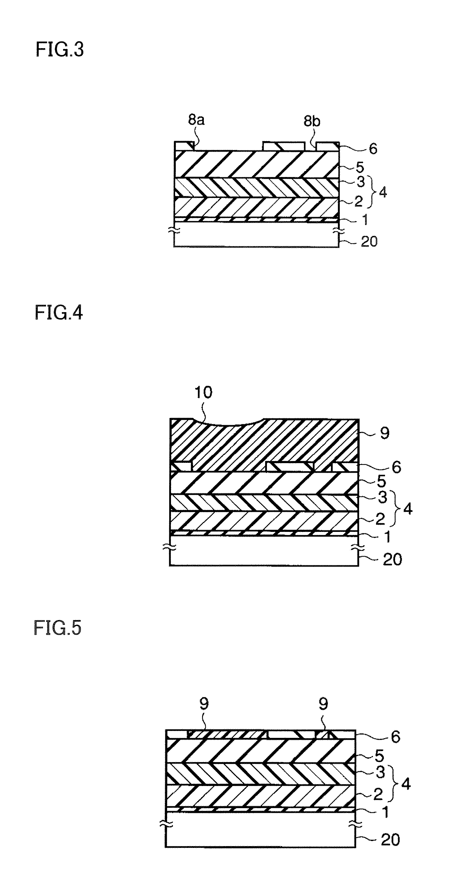
[0135] As shown in FIG. 3, an organic insulating film 4 and the first and second hard masks 5 and 6 including an inorganic material were formed in that order on a semiconductor substrate 20 on which an element (not shown) was formed. The interconnect groove patterns 8a and 8b as depressions were formed in the second hard mask 6. In the example shown in FIG. 3, the organic insulating film 4 has a two-layer structure formed of a first organic insulating film 2 and a second organic insulating film 3. An etching stopper film 1 is formed in the lower layer of these films.

[0136] An interlayer dielectric (not shown) in which a first interconnect layer is formed is provided...

example 2

2-3. Example 2

[0167] In this example, hybrid dual damascene processing by a dual hard mask method using an ArF excimer laser incorporating planarization of an organic film by CMP was performed in the same manner as in Example 1.

[0168] In this example, the first organic film 9 was chemically and mechanically polished using the above slurry 3.

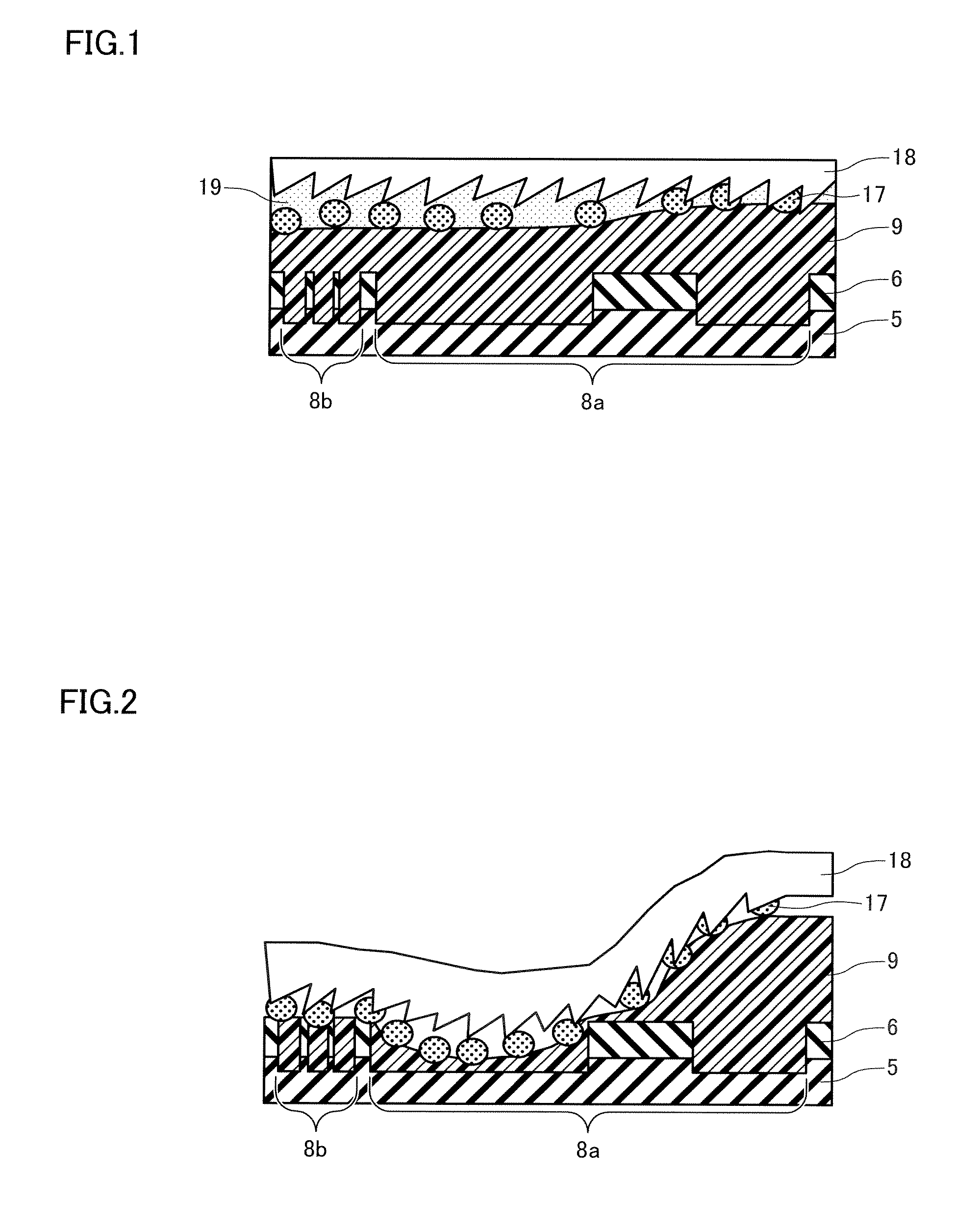
[0169] In more detail, the interconnect groove patterns 8a and 8b were formed in the second hard mask 6 (SiN film) using the method described in Example 1. The first organic film 9 was formed by coating and planarized by CMP.

[0170] In this example, the first organic film 9 was planarized using the device, polishing pad, load, and rotational speed described in Example 1 except for using the slurry 3 as the CMP slurry. Specifically, a slurry (slurry 3) was used which was produced by mixing crosslinked PST particles (crosslinked polymer particles) (abrasive) with an average particle diameter of 50 nm, which was smaller than that of the polymer pa...

example 3

2-10. Example 3

[0193] In this example, hybrid dual damascene processing was performed by a dual hard mask method using an ArF excimer laser incorporating planarization of an organic film by CMP.

[0194] In Example 1, two organic films were used as the lower-layer film 12. In Example 1, the resist containing a novolac resin as the main component (IX370G manufactured by JSR Corporation) was applied to form the first organic film 9. After planarizing the first organic film 9 by CMP, CT01 was applied to form the second organic film 11. This aims at improving the lithographic performance by using IX370G (first organic film 9) which exhibits excellent embedding characteristics and planarization characteristics and CT01 (second organic film 11) which can function as the anti-reflective film during lithography using an ArF excimer laser in combination.

[0195] In this example, the organic film 9 containing a novolac resin as the main component (ODL-50 manufactured by JSR Corporation) was used...


PUM


Abstract

A chemical mechanical polishing method comprises polishing an organic film using a slurry including polymer particles having a surface functional group and a water-soluble polymer.

Description

[0001] Japanese Patent Application No. 2005-345790 filed on Nov. 30, 2005, is hereby incorporated by reference in its entirety. BACKGROUND OF THE INVENTION [0002] The present invention relates to a chemical mechanical polishing method and a method of manufacturing a semiconductor device. [0003] In the manufacturing process of semiconductor devices, a resist film is used to form a desired structure. The resist film is required to have a uniform thickness over the entire wafer. For example, a desired structure is obtained by forming a trench in a semiconductor substrate or a hole in an insulating film, applying a photoresist to form a resist film, and recessing or removing the resist film. [0004] In this case, the resist film is required to have a uniform thickness over the entire wafer. [0005] A variation in thickness of the resist film is increased during the subsequent recess step to cause the device shape to deteriorate. Moreover, a decrease in depth of focus or yield occurs. [000...

Claims


Application Information

Patent Timeline
IPC IPC(8): H01L21/4763H01L21/461B24B37/00H01L21/304
CPCC09G1/02H01L21/31058H01L21/31144H01L21/7681H01L21/76835C09K3/14
Inventor SHIDA, HIROTAKAMATSUI, YUKITERUSHIGETA, ATSUSHIHIRASAWA, SHINICHIKATO, HIROKAZUKINOSHITA, MASAKONISHIOKA, TAKESHIYANO, HIROYUKI
Owner JSR CORPORATIOON
Why Eureka
Try Eureka