

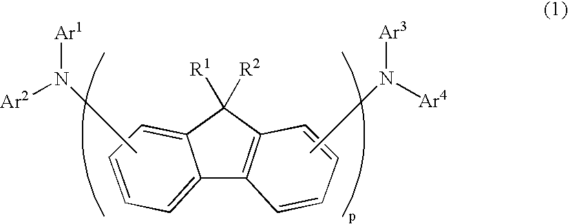
Organic electroluminescence device
a technology of electroluminescent devices and organs, which is applied in the direction of thermoelectric devices, discharge tubes luminescnet screens, natural mineral layered products, etc., can solve the problems of short lifetime, thermal decomposition, and inability to achieve the level of practical use of emission efficiency and lifetim
- Summary
- Abstract
- Description
- Claims
- Application Information
AI Technical Summary
Benefits of technology
Problems solved by technology
Method used
Image


Examples
example 1
(1) Fabrication of Organic EL Device
[0182] A 120 nm thick transparent electrode made of indium tin oxide was formed on a glass substrate measuring 25×75×1.1 mm. The glass substrate was subjected to ultrasonic cleaning in isopropyl alcohol and cleaned by irradiating UV rays and ozone.
[0183] Next, the transparent glass substrate with the transparent electrode was set up on a substrate holder in a deposition chamber of a vacuum deposition device. After the degree of vacuum in the vacuum chamber was reduced to 1×10⁻³ Pa, a hole-injecting layer, a hole-transporting layer, an emitting layer, an electron-transporting layer, an electron-injecting layer and a cathode layer were stacked in sequence on an anode layer under the following conditions to fabricate an organic EL device.
Hole-injecting layer: N′,N″-bis[4-(diphenylamino)phenyl]-N′,N″-diphenylbiphenyl-4,4′-diamine (TPD232)
[0184] Deposition conditions; 2 nm / sec, thickness 60 nm
Hole transporting layer: N,N-bis[4′-{N-(naphthyl-1-y...
examples 2 to 4
[0192] In Examples 2 to 4, organic EL devices were fabricated in the same manner as in Example 1 except that the following hosts and dopants were used for an emitting layer instead of the host (ANI) and the dopant (AFII) used in Example 1. They were evaluated in the same manner as in Example 1 and the results obtained were shown in Table 1.
example 2
(1) Example 2
[0193] Deposition conditions of the host (PYI); 4 nm / sec
[0194] Deposition conditions of the dopant (AFII); 0.2 nm / sec thickness 40 nm ((PYI):(AFII)=40:2)
PUM
| Property | Measurement | Unit |
|---|---|---|
| weight % | aaaaa | aaaaa |
| transmittance | aaaaa | aaaaa |
| work function | aaaaa | aaaaa |
Abstract
Description
Claims
Application Information