[0010]An
advantage of some aspects of the invention is that an emissive device has
uniform quality in each pixel and enhanced
directivity of pencils of light radiating to the outside. Another
advantage of some aspects of the invention is that an electronic apparatus includes the emissive device.
[0012]According to an aspect of the invention, the light-transmitting portions of the light-shielding layer overlap the respective openings in the partition partitioning the light-emitting elements and each are smaller than the corresponding opening. Thus, pencils of light viewable from the outside are regulated by the light-transmitting portions of the light-shielding layer. The light-shielding layer masks peripheries of pixels. Even when luminance and
chromaticity at the peripheries of the pixels close to the partition differ from those at middle portions of the pixels remote from the partition, nonuniformity in luminance and
chromaticity in a
single pixel is not visually identified because the peripheries of the pixels are masked with the light-shielding layer. Furthermore, the light-transmitting portions of the light-shielding layer overlap the respective opening in the partition partitioning the light-emitting elements and are each smaller than the corresponding opening. Thus, it is possible to enhance the
directivity of the pencils of light radiating to the outside.
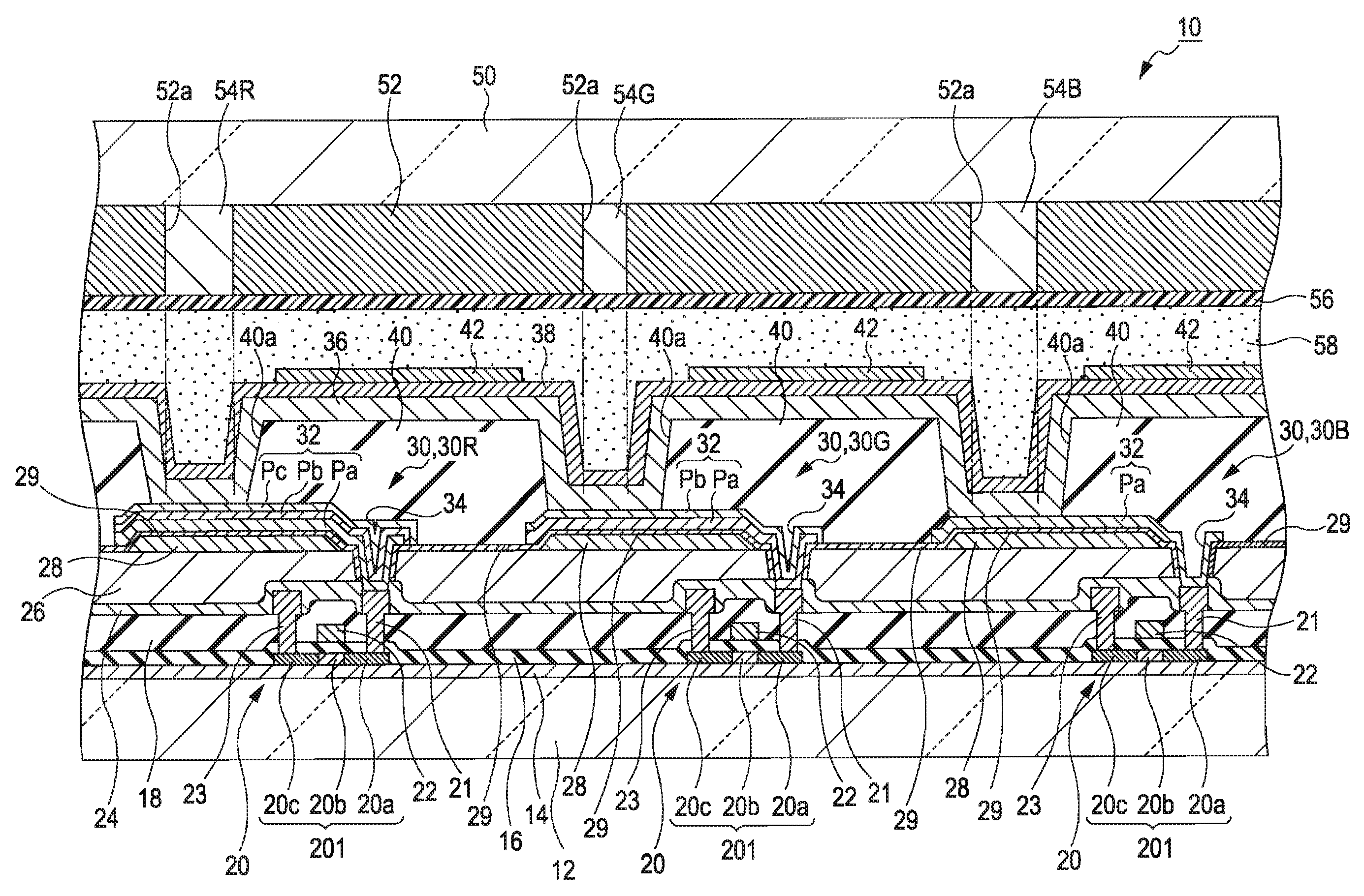
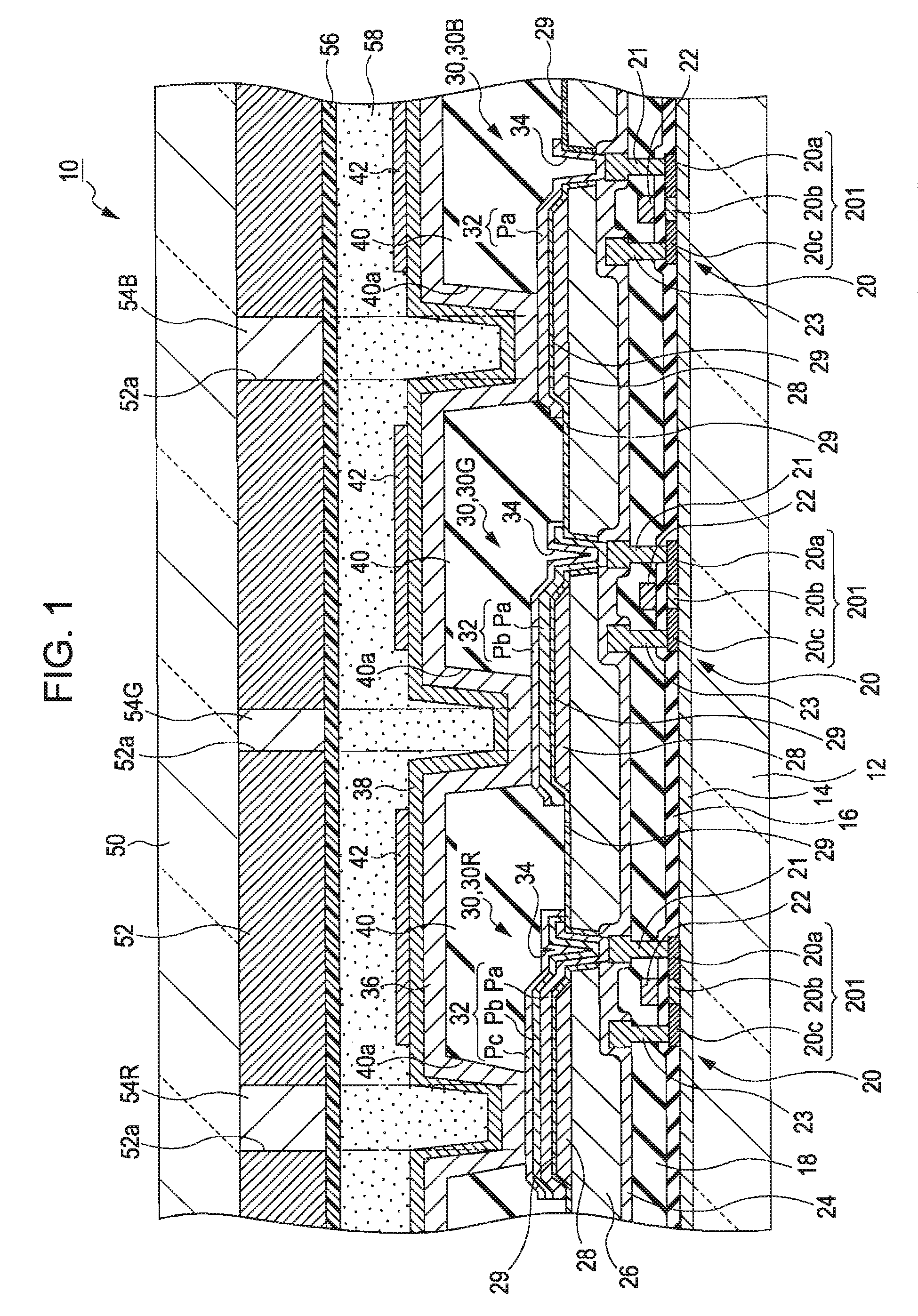
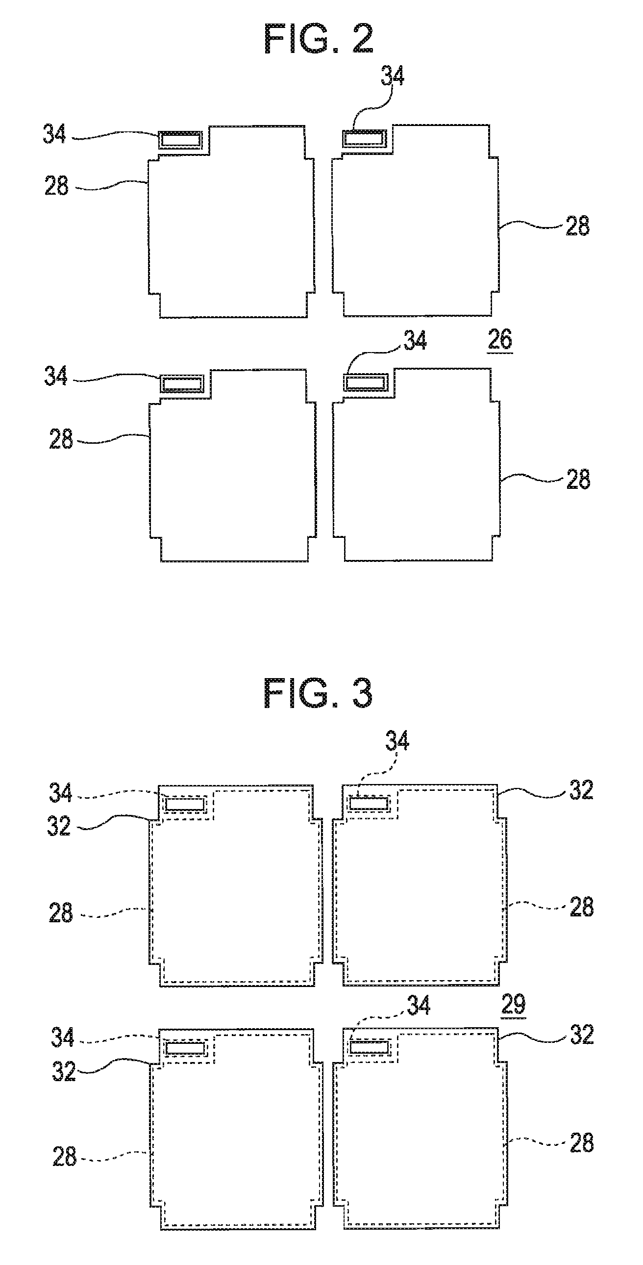
[0014]Preferably, the above-described emissive device further includes first electrodes; a second
electrode; and a light-emitting sublayer disposed between the second
electrode and the individual first electrodes, wherein each of the first electrodes is closer to the corresponding
reflective layer than the second
electrode, is composed of
indium tin oxide (ITO),
indium zinc oxide (IZO), or ZnO2, overlaps the corresponding
reflective layer, and is wider than the corresponding
reflective layer. A
conductive oxide material, such as ITO, IZO, or ZnO2, having light transparency and
conductivity can be used as electrodes for the light-emitting elements. Thus, the
conductive oxide material can transmit light from the light-emitting elements to the reflective
layers and can transmit light reflected from the reflective
layers in the opposite direction. The first electrodes each composed of the
conductive oxide material are patterned by
etching with a strong acid, such as
hydrogen bromide or
hydrogen iodide. The reflective
layers are each composed of a
metal, such as aluminum, or other material having
high reflectivity. Since each of the first electrodes overlaps the corresponding reflective layer and is wider than the corresponding reflective layer, it is possible to prevent the failure of the reflective layers caused by the use of a strong acid.
[0015]Preferably, color conversion layers for converting the color of light emitted from the light-emitting elements into different target colors are disposed at the respective light-transmitting portions, wherein the color conversion layers providing different target colors have different areas. Each of the color conversion layers may be a color filter that transmits more light of a predetermined
wavelength range than light of other
wavelength ranges. Alternatively, each of the color conversion layers may be composed of a photoluminescent material that receives light to emit another color of light.
Luminous energy of the light-emitting elements is not uniform with respect to wavelengths of all colors. Degrees of conversion efficiency of the color conversion layers are different in response to the target colors. The term “conversion efficiency” means the ratio of the luminance of light incident on the color conversion layer to the luminance of outgoing light from the color conversion layer. Thus, even when a constant
driving current is applied to light-emitting elements which have the same size and the same structure, the degrees of luminance of light converted through the color conversion layers are different in response to the types of color conversion layers, i.e., target colors. In consideration of spectrum properties of light incident on the color conversion layers and the conversion efficiency of the color conversion layers,
luminous intensity (unit:
candela), which is the product of luminance and an area, of each light-emitting element can be suitably set by changing the area of the corresponding color conversion layer in response to the target colors. Thereby, it is possible to improve
image quality by striking a balance among the target colors.

