pH buffered aqueous cleaning composition and method for removing photoresist residue

Active Publication Date: 2007-07-12
VERSUM MATERIALS US LLC
View PDF52 Cites 21 Cited by
  • Summary
  • Abstract
  • Description
  • Claims
  • Application Information

AI Technical Summary

Benefits of technology

[0016] In a second aspect of the invention, there is provided a method of removing residue from a substrate comprising contacting the

Problems solved by technology

However, compositions that were once suitable for cleaning state of the art semiconductor materials are not as suitable for use with more recently developed materials, such as organosilica glass (OSG) dielectrics and other low-k dielectrics.
Organic solvents can be unsuitable for use with certain low-k diele

Method used


Image

  • pH buffered aqueous cleaning composition and method for removing photoresist residue
  • pH buffered aqueous cleaning composition and method for removing photoresist residue

Examples


Embodiment Construction

[0018] A composition and method comprising same for selectively removing residues from a substrate are disclosed herein. The composition disclosed herein is capable of selectively removing a residue, such as processing residue, from a substrate without attacking (to any undesired extent) structural materials of the substrate that might also be exposed to the composition.

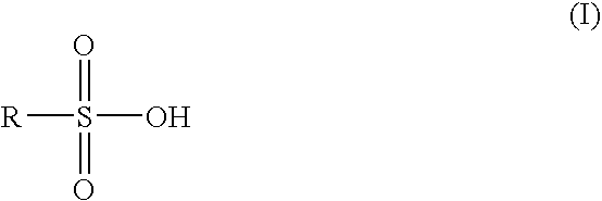
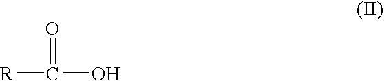
[0019] As used herein, the term “residue” denotes an undesirable material present on the substrate. Residues that can be removed by the invention include but are not limited to: organic compounds, such as exposed and ashed photoresist material; ashed photoresist residue; UV- or X-ray-hardened photoresist; C-F-containing polymers; low and high molecular weight polymers and other organic etch residues; inorganic compounds such as metal oxides; ceramic particles from chemical mechanical planarization (CMP) slurries and other inorganic etch residues; metal containing compounds such as organometallic residues and metal o...


PUM

PropertyMeasurementUnit
Temperatureaaaaaaaaaa

Abstract

A residue cleaning composition includes: (a) water; (b) a fluoride; (c) a pH buffer system including an organic acid and a base. The organic acid can be an aminoalkylsulfonic acid and/or an aminoalkylcarboxylic acid. The base can be an amine and/or a quaternary alkylammonium hydroxide. The composition is substantially free of an added organic solvent and has a pH ranging from about 5 to about 12. A method of removing residue from a substrate includes contacting the residue with the cleaning composition. A method for defining a pattern includes etching the pattern through a photoresist into a substrate, heating the patterned substrate to a temperature sufficient to ash the photoresist and provide a residue, and removing the residue by contacting the residue with the cleaning composition.

Description

BACKGROUND OF THE INVENTION [0001] The invention generally relates to a cleaning composition and process for removal of photoresist residue from semiconductor device substrates after plasma etching and ashing processes in the fabrication of integrated circuits. [0002] Numerous steps are involved in the fabrication of microelectronic structures. Within the manufacturing scheme of fabricating integrated circuits, selective etching of different surfaces of the semiconductor is sometimes required. Historically, a number of vastly different types of etching processes, to selectively remove material, have been successfully utilized to varying degrees. Moreover, the selective etching of different layers, within the microelectronic structure, is considered an important step in the integrated circuit fabrication process. [0003] In the manufacture of semiconductors and semiconductor microcircuits, it is frequently necessary to coat substrate materials with a polymeric organic substance. Examp...

Claims


Application Information

Patent Timeline
IPC IPC(8): C11D7/32
CPCC11D3/046H01L21/02071C11D3/28C11D3/30C11D3/33C11D3/349C11D7/10C11D7/28C11D7/3209C11D7/3245C11D7/3281C11D7/34C11D11/0047G03F7/425G03F7/426H01L21/02063C11D3/245
Inventor WU, AIPINGROVITO, ROBERTO JOHN
Owner VERSUM MATERIALS US LLC
Why Eureka
Try Eureka