Three-dimensional control-gate architecture for single poly EPROM memory devices fabricated in planar CMOS technology

a technology of planar cmos and control gate, which is applied in the direction of semiconductor devices, electrical equipment, instruments, etc., can solve the problems of large cell area limitation of single-poly cmos non-volatile semiconductor memory (nvsm) designs, insufficient capacitance of gate oxide that is thermally grown on heavily doped silicon regions, and insufficient gate oxide quality to provide capacitance. , to achieve the effect of increasing the coupling ratio of a control ga

Active Publication Date: 2007-07-19
TOWER SEMICONDUCTOR
View PDF12 Cites 62 Cited by
  • Summary
  • Abstract
  • Description
  • Claims
  • Application Information

AI Technical Summary

Benefits of technology

[0008] Accordingly, the present invention provides a three-dimensional capacitor structure that combines various types of capacitance, including polysilicon-to-substrate capacitance, contact-to-polysilicon ...

Problems solved by technology

The main limitation of single-poly CMOS non-volatile semiconductor memory (NVSM) designs is a large-cell area.
The above-listed devices require special lithography and ion implant doping steps that must be performed before the gate...

Method used


Image

  • Three-dimensional control-gate architecture for single poly EPROM memory devices fabricated in planar CMOS technology
  • Three-dimensional control-gate architecture for single poly EPROM memory devices fabricated in planar CMOS technology
  • Three-dimensional control-gate architecture for single poly EPROM memory devices fabricated in planar CMOS technology

Examples


Embodiment Construction

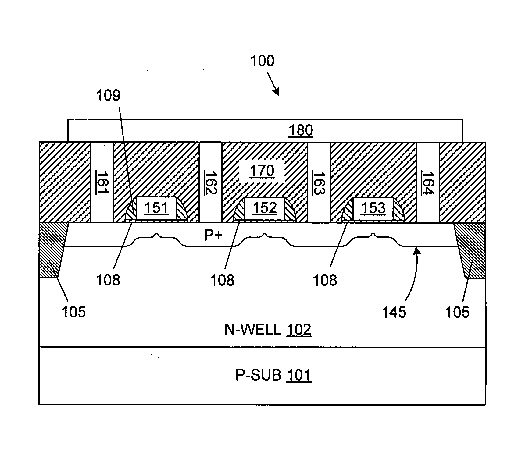
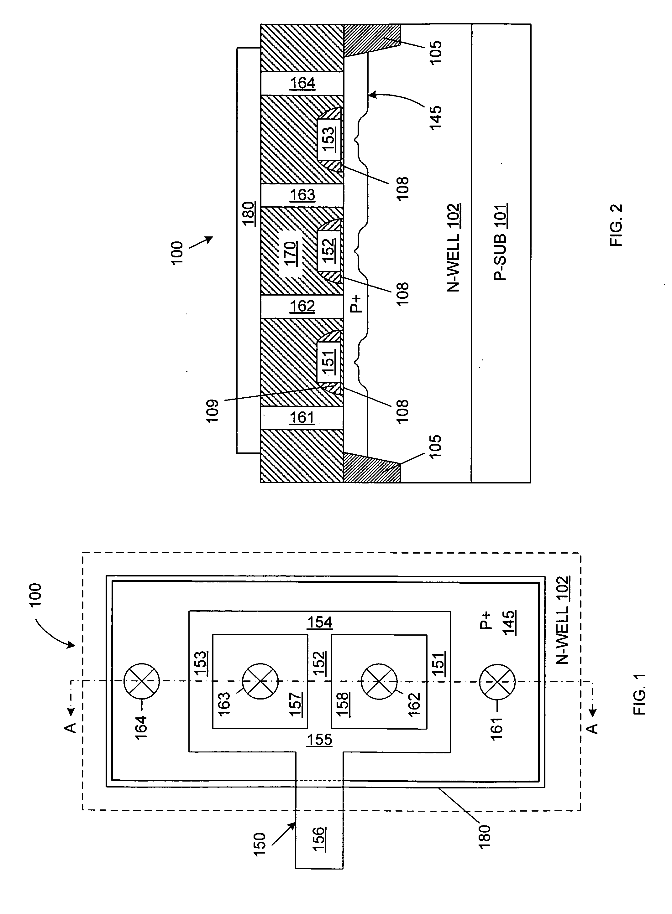
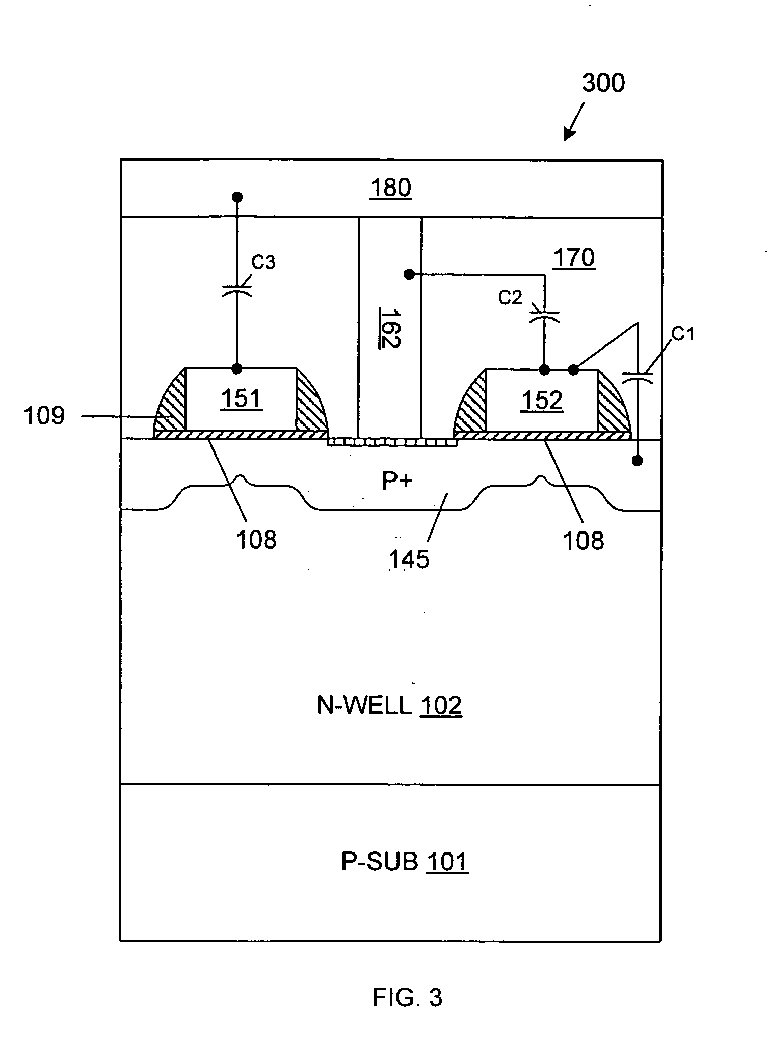
[0026]FIG. 1 is a top view of a capacitor structure 100, which can be used to implement a three dimensional control gate of a single-poly non-volatile memory (NVM) cell, in accordance with one embodiment of the present invention. FIG. 2 is a cross-sectional view of capacitor structure 100 along section line A-A of FIG. 1. As used herein, a single-poly NVM cell includes any NVM cell fabricated with a single polysilicon gate layer. This single polysilicon gate layer is used to form the floating gates of the NVM cells, as well as the control gates of other transistors fabricated on the same wafer. Capacitor structure 100 can be used, for example, to implement the control gate of an electrically programmable erasable read only memory (EEPROM) cell or a compact flash memory cell.

[0027] Capacitor structure 100 includes p-type monocrystalline semiconductor (e.g., silicon) substrate 101, n-type well region 102, field dielectric regions 105, capacitor dielectric layer 108, dielectric sidewa...


PUM


Abstract

A capacitor for a single-poly floating gate device is fabricated on a semiconductor substrate along with low and high voltage transistors. Each transistor has a gate width greater than or equal to a minimum gate width of the associated process. A dielectric layer is formed over the substrate, and a patterned polysilicon structure is formed over the dielectric layer. The patterned polysilicon structure includes one or more narrow polysilicon lines, each having a width less than the minimum gate width. The LDD implants for low and high voltage transistors of the same conductivity type are allowed to enter the substrate, using the patterned polysilicon structure as a mask. A thermal drive-in cycle results in a continuous diffusion region that merges under the narrow polysilicon lines. Contacts formed adjacent to the narrow polysilicon lines and a metal-1 trace connected to the contacts may increase the resulting capacitance.

Description

FIELD OF THE INVENTION [0001] The present invention relates to an EEPROM control gate fabricated using a standard planar CMOS fabrication process. RELATED ART [0002] The main limitation of single-poly CMOS non-volatile semiconductor memory (NVSM) designs is a large-cell area. One option to decrease the cell area is to form a control gate of the cell in the substrate. A single-poly non-volatile memory device using p-type and n-type doped layers underneath a single-poly gate layer has been described. Kwok et al., “An Innovative NVM Technology for Sub-0.25 um SOC Applications”, CASPA / CIE System-on-Chip (SOC) Symposium May 16, 1998, pp. 1-24. [0003] Nae-In Lee et al. report an EEPROM device that uses a PMOS transistor structure as the control gate for a NMOS EEPROM device. Lee et al., “High-Performance EEPROM's Using N- and P-Channel Polysilicon Thin-Film Transistors with Electron Cyclotron Resonance N20-Plasma Oxide”, IEEE Electron Device Letters, Vol. 20, No. 1, January 1999, pp. 15-1...

Claims


Application Information

Patent Timeline
IPC IPC(8): H01L21/8244
CPCG11C16/0408G11C2216/10H01L27/105H01L29/94H01L27/11526H01L27/11558H01L29/7833H01L27/11521H10B41/60H10B41/40H10B41/30
Inventor FENIGSTEIN, AMOSKURITSKY, ZOHARLAHAV, ASAFNAOT, IRAROIZIN, YAKOV
Owner TOWER SEMICONDUCTOR
Why Eureka
Try Eureka