Indium oxide based material and method for preparing the same
a technology of indium oxide and based materials, which is applied in the direction of oxide conductors, conductors, non-metal conductors, etc., can solve the problems of insufficient practice use resistance reduction, and achieve the effect of increasing the electrical conductivity and light transmittance of the indium oxide or indium oxide based material, and increasing the electrical conductivity and light transmittan
- Summary
- Abstract
- Description
- Claims
- Application Information
AI Technical Summary
Benefits of technology
Problems solved by technology
Method used
Image
Examples
example 1
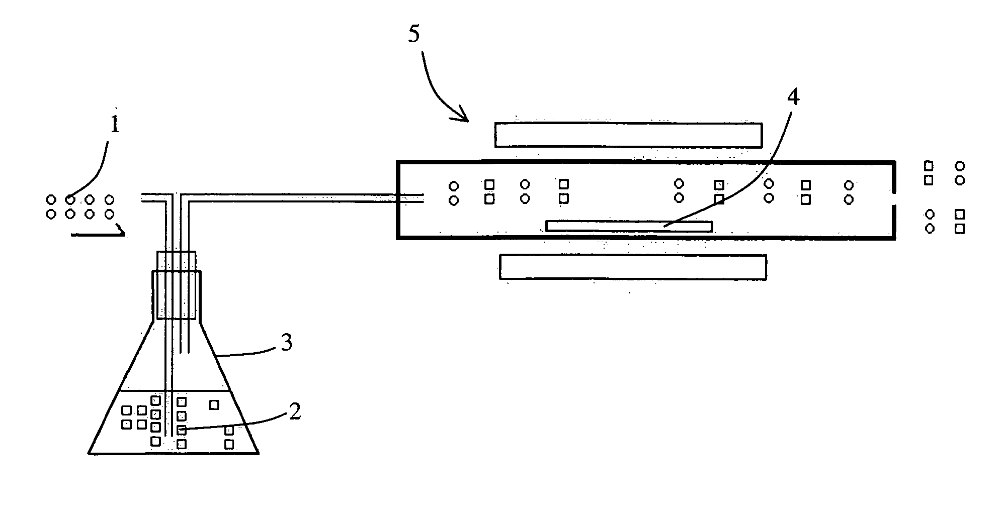
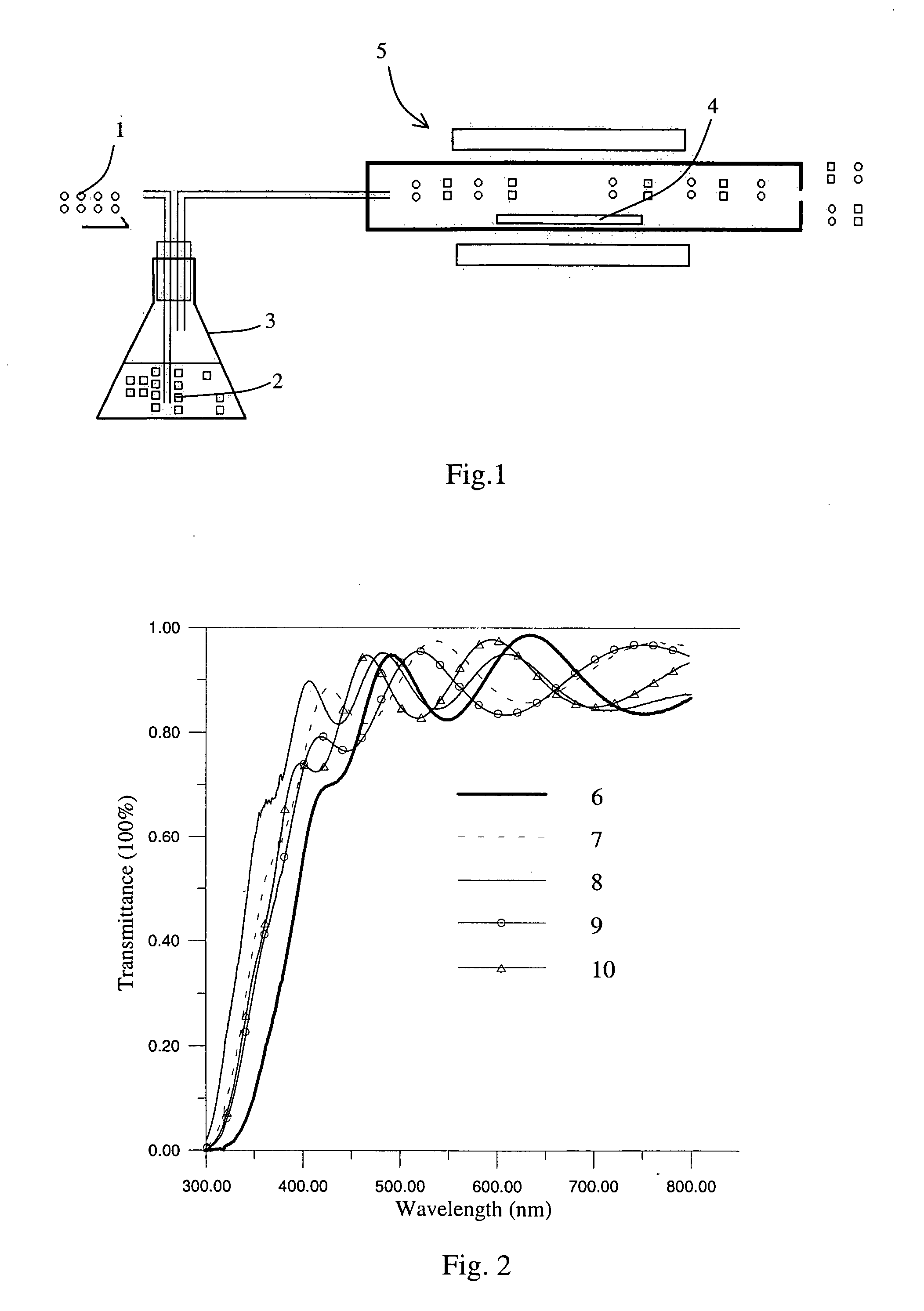
[0029] The nitrogen gas and the oxygen gas are respectively introduced to the annealing system as shown in FIG. 1, and the nitrogen gas is also introduced to the container containing ethanol or ammonia water, and then a gas mixture of ethanol vapor or ammonia water vapor, and nitrogen gas is obtained by bubbling nitrogen gas through the container. The gas mixture is then introduced to the annealing system in which the indium tin oxide film sputtered at 25° C. has been disposed. Subsequently, the annealing process is carried out at 300° C. for one hour. The light transmittances of the indium tin oxide films without annealing and with annealing in different gases are respectively measured by a UV / VIS / NIR spectrometer, as shown in FIG. 2.
[0030] Referring to FIG. 2, the transmittance edge of the indium tin oxide film annealed under the flow of the gas mixture of ethanol vapor in nitrogen shifts toward the shorter wavelength side (blue shift) in comparison with the indium tin oxide film...
example 2
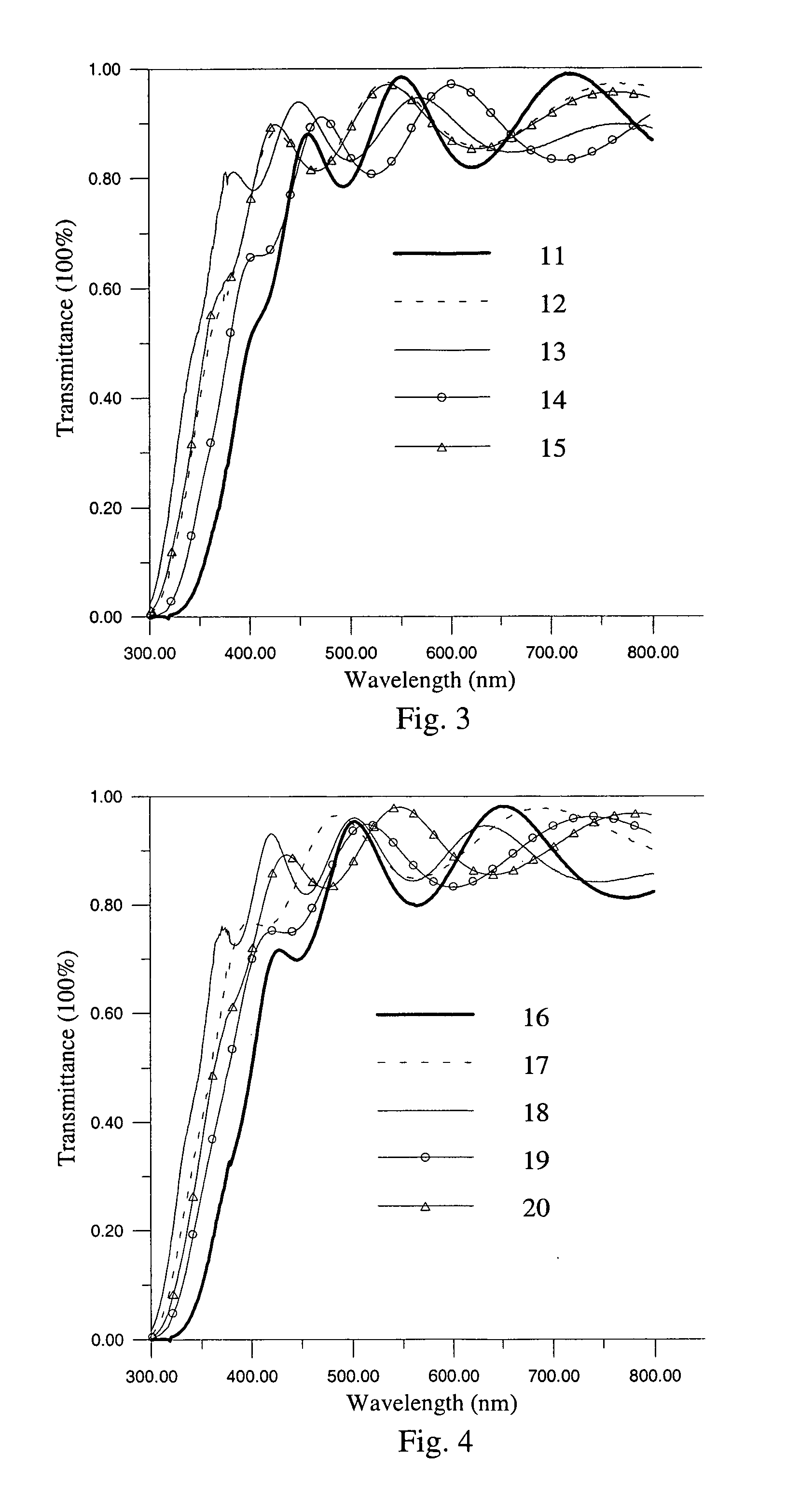
[0031] The same measurement method and conditions as in Example 1 are used except that the indium tin oxide films are respectively formed on a substrate by sputtering at 100° C., 200° C., 250° C., and 300° C. instead of 25° C. The light transmittances of the indium tin oxide films treated under the same conditions as in Example 1 are respectively measured by a UV / VIS / NIR spectrometer. These measured light transmittances are respectively shown in FIG. 3, FIG. 4, FIG. 5, and FIG. 6. In FIG. 3, FIG. 4, FIG. 5, and FIG. 6, the reference numerals 11, 16, 21, 26 represent without annealing; the reference numerals 12, 17, 22, 27 represent the introduction of pure nitrogen to the annealing system; the reference numerals 13, 18, 23, 28 represent the introduction of ethanol in nitrogen to the annealing system; the reference numerals 14, 19, 24, 29 represent the introduction of pure oxygen to the annealing system; and the reference numerals 15, 20, 25, 30 represent the introduction of ammonia ...
example 3
[0034] The same measurement method and conditions as in Example 1 are used except that methanol, ethanol, or acetone is placed in a container. The light transmittances of the indium tin oxide films treated under the same conditions as in Example 1 are respectively measured by a UV / VIS / NIR spectrometer. These measured light transmittances for the indium tin oxide films annealed under the flow of methanol vapor in nitrogen, ethanol vapor in nitrogen, and acetone vapor in nitrogen are respectively shown in FIG. 7. In FIG. 7, the reference numeral 31 represents the introduction of methanol in nitrogen to the annealing system; the reference numeral 32 represents the introduction of ethanol in nitrogen to the annealing system; and the reference numeral 33 represents the introduction of acetone in nitrogen to the annealing system.
[0035] As seen from FIG. 7, the transmittance edges of the indium tin oxide films respectively annealed under the flow of the gas mixture of methanol vapor in ni...
PUM
| Property | Measurement | Unit |
|---|---|---|
| transmittable wavelengths | aaaaa | aaaaa |
| transmittable wavelengths | aaaaa | aaaaa |
| boiling point | aaaaa | aaaaa |
Abstract
Description
Claims
Application Information


