Method of fabricating a composite substrate with improved electrical properties

Active Publication Date: 2007-07-26
S O I TEC SILICON ON INSULATOR THECHNOLOGIES
View PDF8 Cites 32 Cited by
  • Summary
  • Abstract
  • Description
  • Claims
  • Application Information

AI Technical Summary

Benefits of technology

[0015] The present invention overcomes the disadvantages of the prior art by providing new and useful methods of producing a composite substrate that includ

Problems solved by technology

A trap can have an extremely deleterious impact on electrical properties of any future electronic components produced on the composite substrate.
The higher the DIT value, the worse the electrical properties of the substrate.
Thus, the FGA treatment method loses effectiveness at each encountered interface.
Thus, FGA treatment is relatively ineffective for deep-lying interfaces.
This treatment cannot be applied to certain structures formed by bonding, or to composite substrates containing materials that are unstable at high tempe

Method used


Image

  • Method of fabricating a composite substrate with improved electrical properties
  • Method of fabricating a composite substrate with improved electrical properties
  • Method of fabricating a composite substrate with improved electrical properties

Examples


example 1

[0094] Preparation of a Substrate Including an Active Layer that Comprises a Ground Plane (Known by the Acronym “GP-SOI”, or “Ground Plane Silicon on Insulator”)

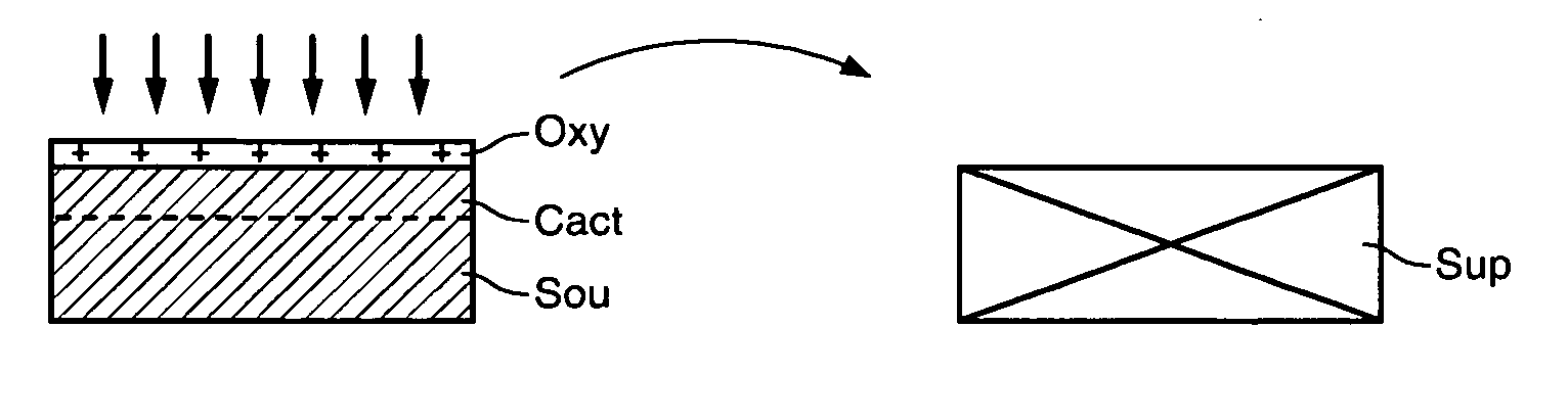
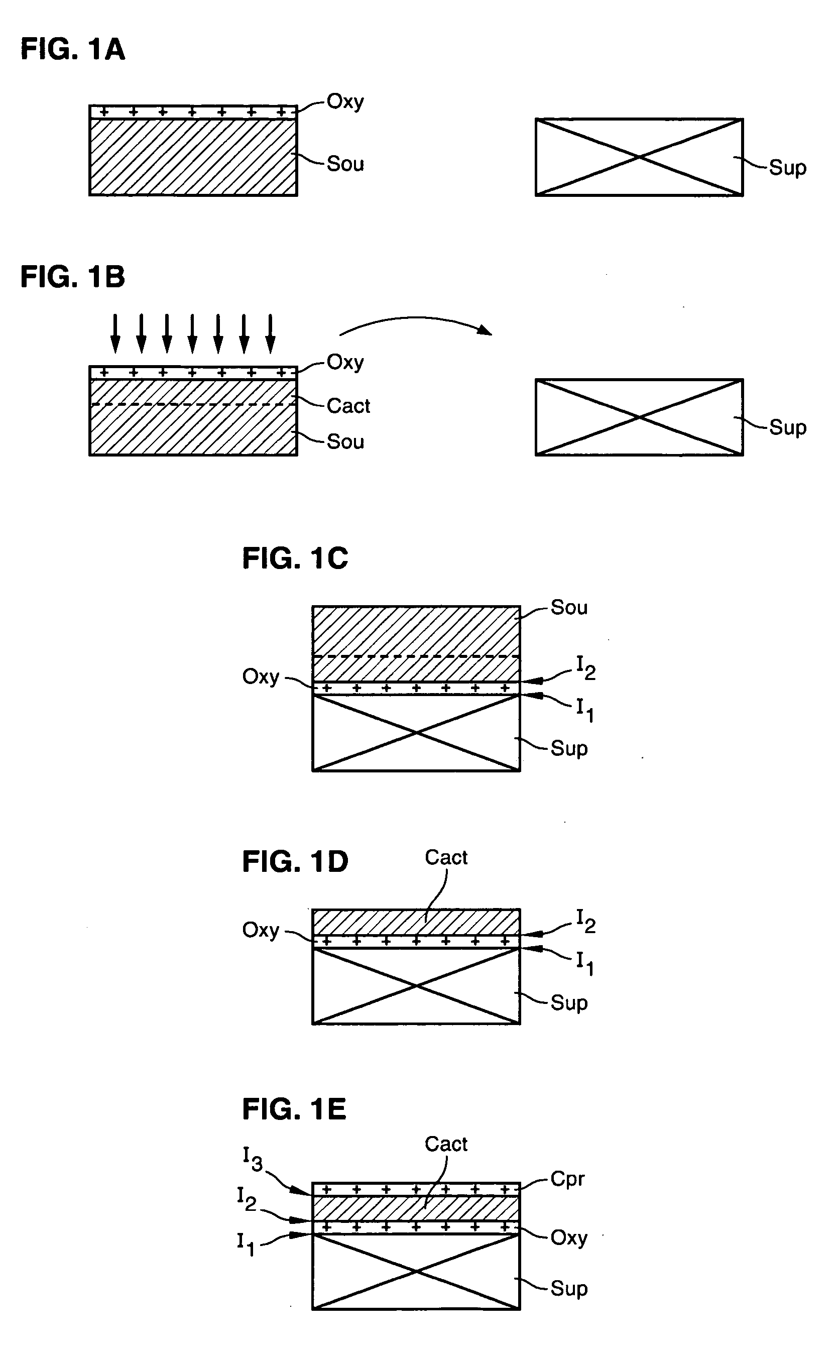
[0095] This example will be described with reference to FIGS. 3A to 3G. A silicon support substrate 1 was covered with a deposit of a thin layer 60 about 1 micrometer (μm) thick and highly doped with boron (see FIGS. 3A and 3B), to define a ground plane therein.

[0096] This highly doped layer had a front face 600 that was used for bonding (see FIG. 3C). Front face 600 was polished or smoothed to reduce its roughness and render front face 600 to render front face 600 compatible with bonding.

[0097] As shown in FIG. 3D, support substrate 1 was covered with a doped layer 60 and then underwent a high temperature thermal annealing treatment or RTA, typically at 1050° C. for about 10 seconds. Further, a silicon source substrate 2 was used, oxidized by dry oxidation.

[0098] Silicon source substrate 2 was covered with a layer 32 of...

example 2

[0103] Preparation of a Composite Substrate Comprising an Active Layer of Silicon on a Stack of Oxide and Quartz

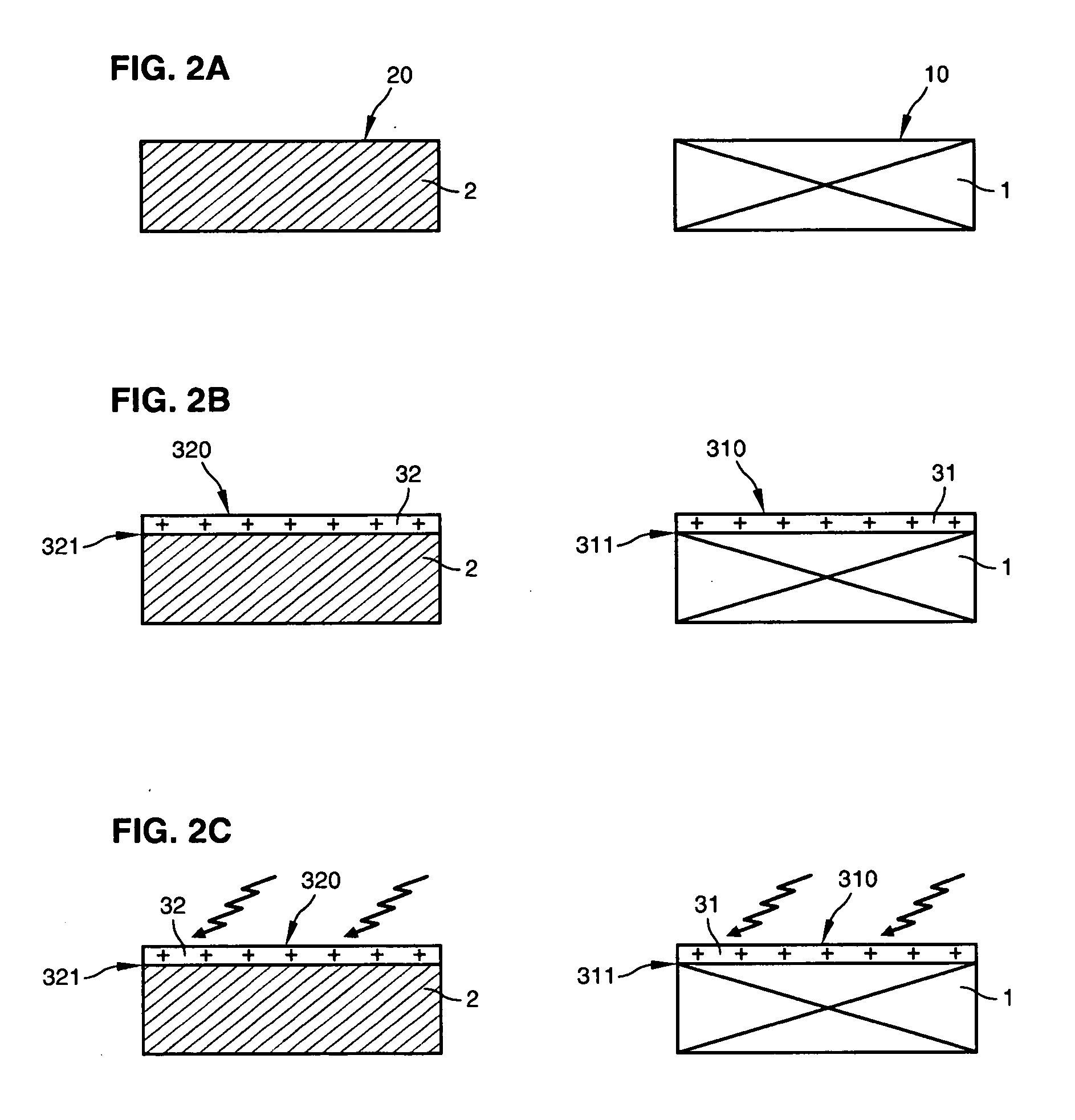
[0104] The same type of source substrate 2 used in Example 1 was employed in Example 2. It underwent the same treatments, with the exception of the recovery treatment that was carried out by a high temperature anneal at 1100° C., and the formation of the zone of weakness was carried out by co-implantation of helium using a dose of 1.5×10¹⁶He+ / cm2 and hydrogen using a dose of 1×10¹⁶H+ / cm2.

[0105] Further, a quartz support substrate 1 comprising a front face 10 that underwent plasma activation using the parameters used in Example 1 for substrate 2 was used.

[0106] The composite substrate thus obtained had DIT values at the interface between the oxide and the silicon of the order of several 1010·eV−1·cm−2.

[0107] In accordance with the invention, the fact that the recovery treatment was carried out systematically prior to plasma activation meant that the bonding energy was n...


PUM


Abstract

The invention concerns a method of fabricating a composite substrate comprising at least one thin insulating layer interposed between a support substrate and an active layer of semiconductor material. The method comprises: providing a source substrate that comprises a semiconductor material and a support substrate; forming or depositing an insulating layer on the source substrate; providing recovery heat treatment of the insulating layer; providing plasma activation of a front face of the recovery heat treated insulating layer or a front face of the support substrate; molecular bonding, after the plasma activation, the front face of the insulating layer with the front face of the support substrate to form a bonded substrate; and lifting off a back portion of the source substrate from the bonded substrate to retain an active layer that comprises a remaining portion of the source substrate.

Description

TECHNICAL FIELD [0001] The present invention relates to a method of low temperature fabrication of a “hybrid” or “composite” substrate of a type comprising at least one buried insulating layer, for example, an insulating layer interposed between a support substrate and an active layer of semiconductor material that can be derived from a source substrate. The invention also relates to a method of obtaining a composite substrate as mentioned above, with substantially improved electrical properties. The substrates described herein can be used in the fields of optics, electronics, and optoelectronics. BACKGROUND ART [0002]FIGS. 1A to 1E illustrate the various steps of one mode of fabricating an SOI type substrate, which is known in the art. [0003] As shown in FIGS. 1A and 1B, the known method consists of oxidizing a source substrate Sou to form a layer of oxide Oxy on a surface of Sou. The method then provides for atomic species implantation in Sou to define an active layer Cact. Oxide ...

Claims


Application Information

Patent Timeline
IPC IPC(8): H01L21/30
CPCH01L21/76256H01L21/76254Y02P70/50H01L21/20H01L21/324
Inventor ALLIBERT, FREDERICKERDILES, SEBASTIEN
Owner S O I TEC SILICON ON INSULATOR THECHNOLOGIES
Why Eureka
Try Eureka