

Negative radiation-sensitive resin composition
- Summary
- Abstract
- Description
- Claims
- Application Information
AI Technical Summary
Benefits of technology
Problems solved by technology
Method used
Image


Examples
synthesis example 1
Synthesis of polymer A1
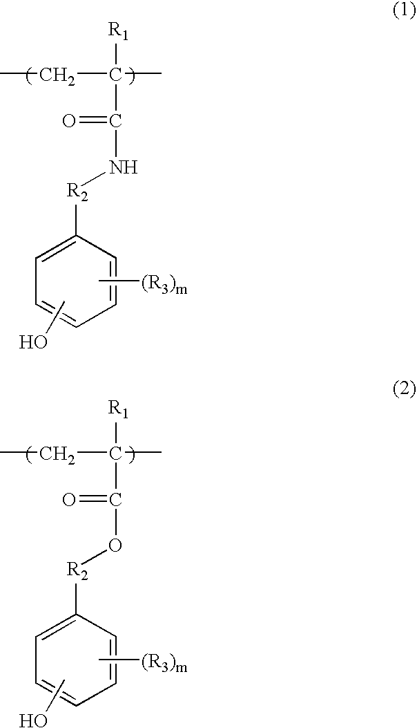
[0139] In a flask equipped with a dry ice / methanol reflux condenser and purged with nitrogen, 5.0 g of 2,2′-azobisisobutyronitrile and 100 g of ethyl lactate were placed, and they were stirred until the polymerization initiator was dissolved. To the solution, 15 g of p-hydroxyphenyl methacrylamide, 5 g of α-methyl-p-hydroxystyrene, 10 g of methacrylic acid, 40 g of n-butyl methacrylate and 30 g of tricyclo[5.2.1.02,6]decanyl methacrylate were added, then stirring was slowly started, and the temperature was raised to 80° C. Thereafter, polymerization was carried out at 80° C. for 6 hours. After the polymerization reaction was completed, the reaction product was dropwise added to a large amount of methanol to solidify the reaction product. The resulting solids were washed with water, then redissolved in the same weight of tetrahydrofuran as that of the solids and dropwise added to a large amount of methanol to perform solidification again. The redissolution and...
synthesis examples 2 to 11
Syntheses of Polymers A2 to A10 and Polymers CA1 to CA2 for Comparison
[0140] Polymers A2 to A10 and CA1 to CA2 were synthesized in the same manner as in “Synthesis of polymer A1” in Synthesis Example 1, except that the types and the amounts of the compounds were changed in accordance with compositions shown in Table 1.
TABLE 1ComponentCopolymerabcdefghiA1155104030A215154030A3155104030A4155104030A5155104030A6155103040A715153040A81010104030A92054035A10254035CA11510302025CA21510302025
a: p-hydroxyphenyl methacrylamide
b: 3,5-dimethyl-4-bezyl acrylamide
c: p-isopropenylphenol
e: 2-hexahydrophthaloylethyl methacrylate
f: n-butyl acrylate
g: n-butyl methacrylate
i: tricyclo[5.2.1.02,6]decanyl methacrylate
example 1
Preparation of Resin Composition
[0141] The polymer A1 (100 g), Aronix M8060 (available from Toagosei Co., Ltd.) (40 g) and dimethylolpropane triacrylate (20 g) as the ethylenically unsaturated compounds (B), 2,2-dimethoxy-1,2-diphenylethane-1-one (15 g), 2,4,6-trimethylbenzoyldiphenylphosphine oxide (3 g) and 2,2′-bis(2,4-dichlorophenyl)-4,5,4′,5′-tetraphenyl-1,2′-bisimidazole (5 g) as the radiation radical polymerization initiators (C), NBX-15 (available from Neos Co. Ltd.) (0.3 g) as a surface active agent and ethyl lactate (90 g) as a solvent were mixed and stirred to give a homogeneous solution. This composition solution was filtered through a capsule filter having a pore diameter of 10 μm to obtain a radiation-sensitive resin composition.
Preparation of Copper Sputtered Substrate
[0142] On a silicone wafer substrate having a diameter of 4 inches, TiW was sputtered in a thickness of about 1000 Å, and thereon was further sputtered copper in a thickness of 3000 Å to form a conduc...
PUM
| Property | Measurement | Unit |
|---|---|---|
| Percent by mass | aaaaa | aaaaa |
| Percent by mass | aaaaa | aaaaa |
| Thickness | aaaaa | aaaaa |
Abstract
Description
Claims
Application Information