Semiconductor device and manufacturing method thereof
- Summary
- Abstract
- Description
- Claims
- Application Information
AI Technical Summary
Benefits of technology
Problems solved by technology
Method used
Image

Examples
Embodiment Construction
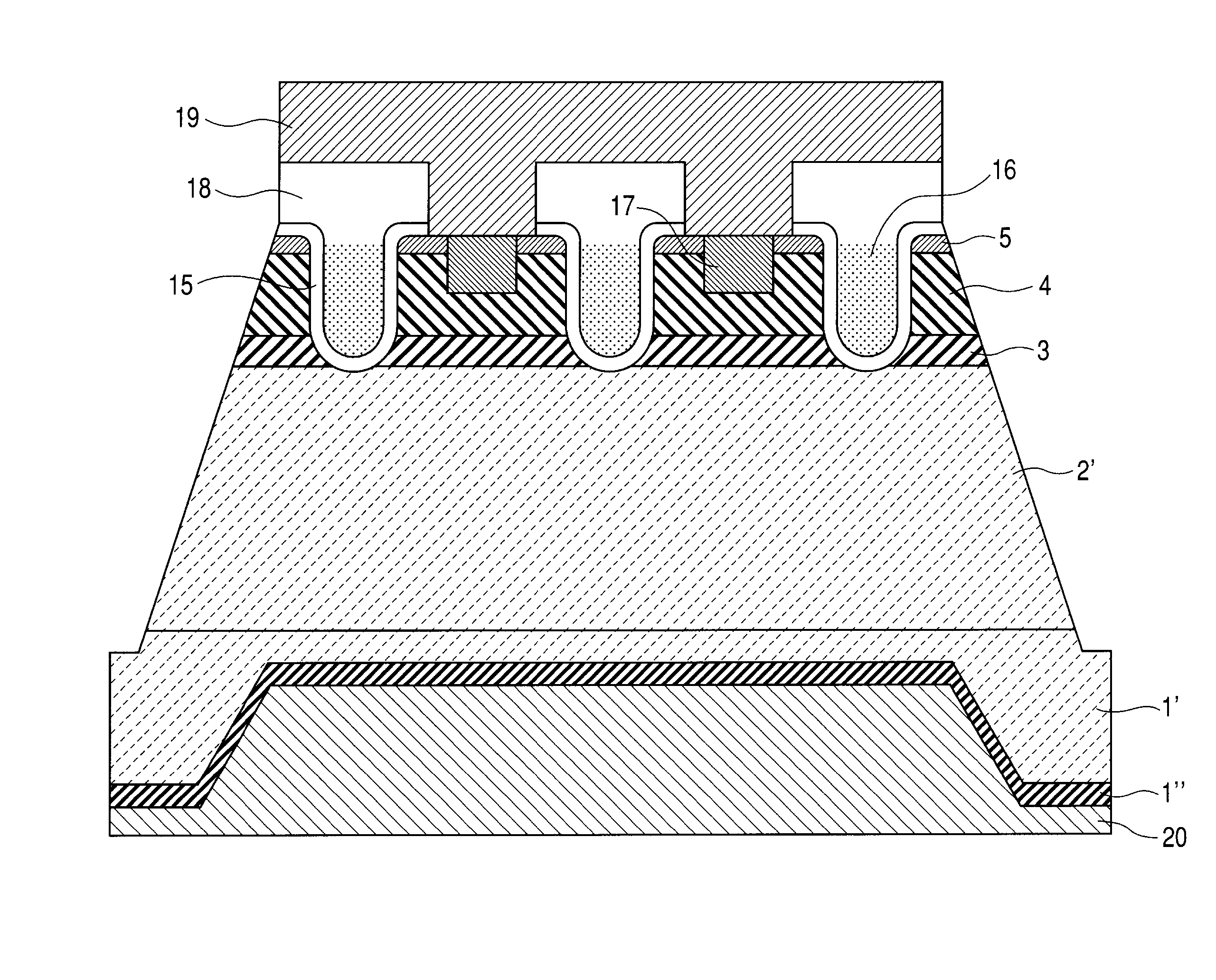
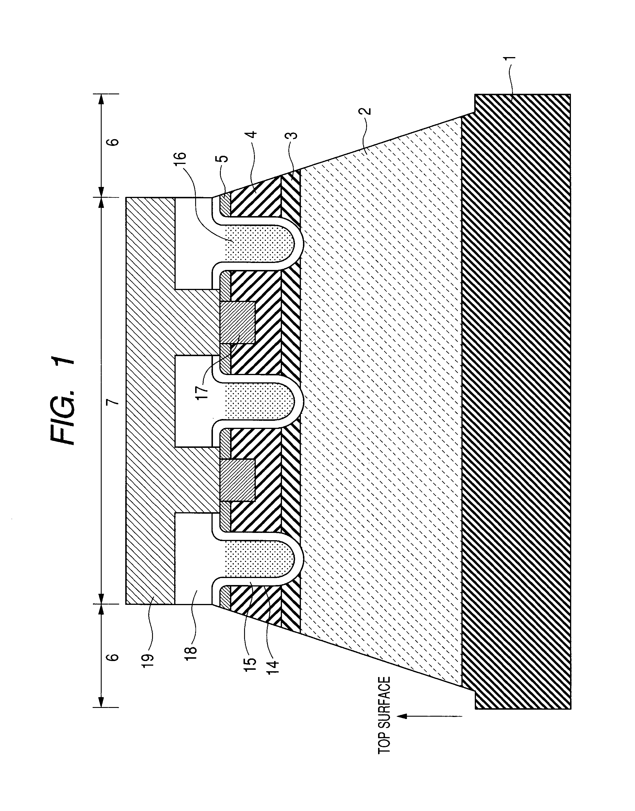
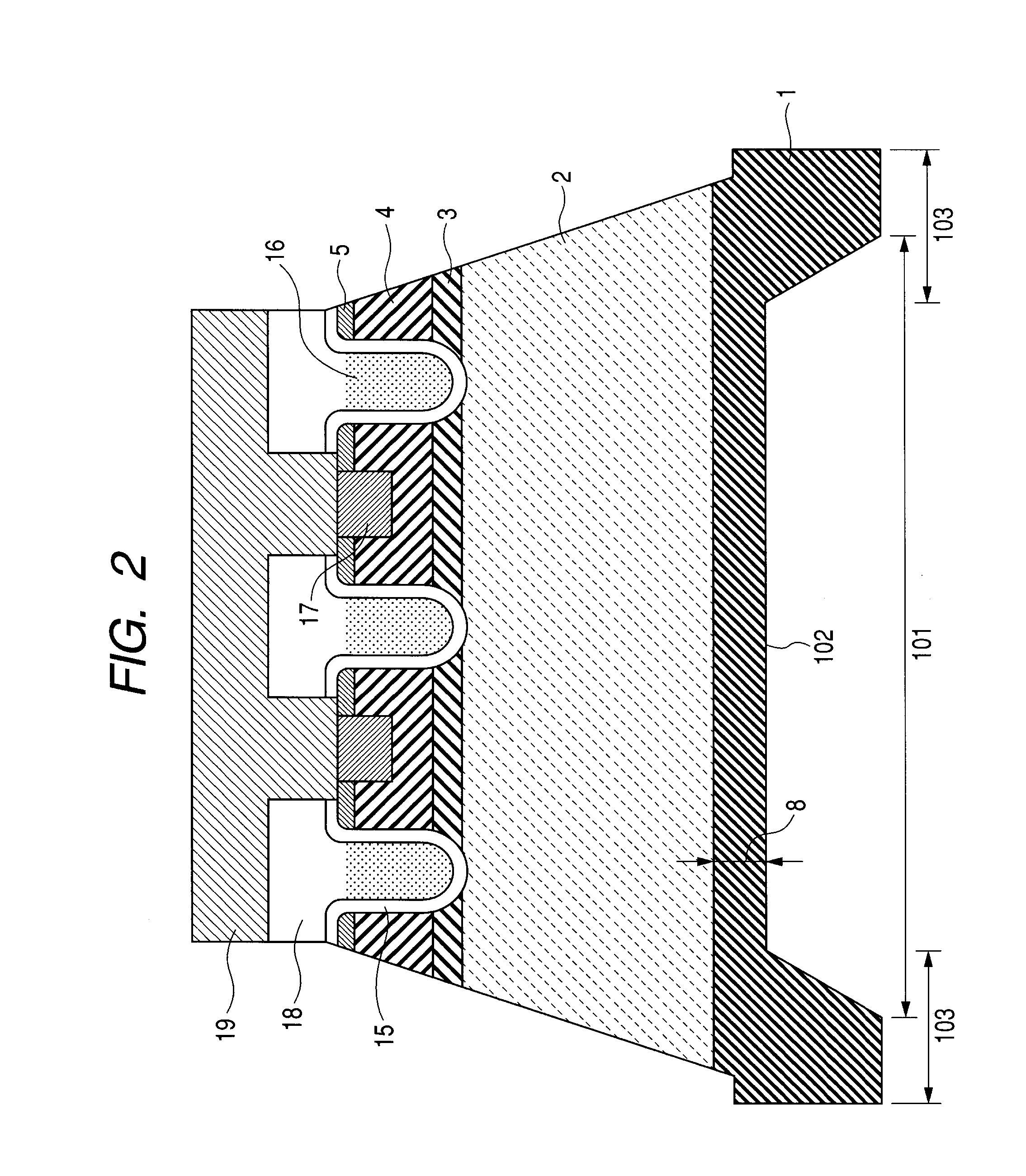
[0034]FIGS. 1-3 are schematic cross-sectional views showing the manufacturing process steps of a first embodiment of a vertical trench MOSFET that uses a silicon carbide substrate. The use of a single crystal substrate of silicon carbide allows the semiconductor layer to be an epitaxially grown layer of silicon carbide or a hetero-epitaxially grown layer of gallium nitride. A single crystal of silicon carbide has various kinds of polytype. For a power semiconductor device, 4H—SiC or 6H—SiC can be used. The semiconductor layer includes any one of a semiconductor layer formed on a semiconductor substrate by epitaxial growth and formed by part of a semiconductor substrate.
[0035] In the first embodiment, a semiconductor device is obtained by epitaxially growing a semiconductor layer of silicon carbide on a semiconductor substrate of silicon carbide. FIGS. 1-3 show cross-sectional views of a vertical trench MOSFET in the order of the manufacturing steps. In the following, explanations w...
PUM
 Abstract
Description
Claims
Application Information
 - Generate Ideas
- Intellectual Property
- Life Sciences
- Materials
- Tech Scout
- Unparalleled Data Quality
- Higher Quality Content
- 60% Fewer Hallucinations
Browse by: Latest US Patents, China's latest patents, Technical Efficacy Thesaurus, Application Domain, Technology Topic, Popular Technical Reports.
© 2025 PatSnap. All rights reserved.Legal|Privacy policy|Modern Slavery Act Transparency Statement|Sitemap|About US| Contact US: help@patsnap.com