Coating liquid for forming organic layered film, method of manufacturing field effect transistor, and field effect transistor

a technology of organic layered film and coating liquid, which is applied in the direction of coatings, solid-state devices, chemistry apparatuses and processes, etc., can solve the problems of contaminants adhering to the insulating layer, mutual dissolution, and not many of them have been put into practical use, so as to improve the carrier mobility of the fet

Inactive Publication Date: 2007-09-20
PANASONIC CORP
View PDF2 Cites 11 Cited by
  • Summary
  • Abstract
  • Description
  • Claims
  • Application Information

AI Technical Summary

Benefits of technology

[0069] A FET of the present invention includes an organic semiconductor layer and an organic insulating layer that adjoins the organic semiconductor layer. At least a part of the organic semiconductor layer functions as a channel region. A source electrode and a drain electrode are disposed so as to be in contact with the organic semiconductor layer.
[0070] The organic semiconductor layer and the organic insulating layer are those formed with the above-mentioned coating liquid. Hence, the organic semiconductor layer is a layer containing, as its main component (preferably at least 95 wt %), the first organic molecules that are an organic semiconductor material. On the other hand, the organic insulating layer is a layer containing, as its main component (preferably at least 95 wt %), the second organic molecules that are an insulator material. The proportion of the first organic molecules decreases gradually from the interface between the organic semiconductor layer and the organic insulating layer toward the outer-side surface of the organic insulating layer. On the contrary, the proportion of the second organic molecules decreases gradually from the interface between the organic semiconductor layer and the organic insulating layer toward the outer-side surface of the organic semiconductor layer.
[0071] Preferably, the content of the first organic molecules in the organic semiconductor layer is at least 50 wt % (preferably at lest 60 wt %) in the vicinity of the interface between the organic semiconductor layer and the organic insulating layer and is at least 95 wt % in the vicinity of the outer-side surface of the organic semiconductor layer. On the other hand, preferably, the content of the second organic molecules in the organic insulating layer is at least 50 wt % (preferably at least 60 wt %) in the vicinity of the interface between the organic semiconductor layer and the organic insulating layer and is at least 95 wt % in the vicinity of the outer-side surface of the organic insulating layer. In this paragraph, the phrase “vicinity of the interface” denotes a region extending up to 10 nm from the interface, while the phrase “vicinity of the surface” means a region extending up to 10 nm from the surface.
[0072] The organic semiconductor layer exhibits its properties even when containing a small amount of organic insulator material. Similarly, the organic insulating layer exhibits its properties even when containing a small amount of organic semiconductor material.
[0073] In the FET of the present invention, the change in concentration of the constituent molecules in the direction from the interface between the semiconductor layer and the insulating layer toward the semiconductor layer is gradual as compared to the case where the semiconductor layer and the insulating layer are produced individually through respective solution applications. Generally, the carrier trapping level density in the region where the element concentration changes gradually is lower than that in the region where the concentration changes sharply. Hence, the trapping level density at the interface between the semiconductor layer and the insulating layer of the FET according to the present invention is lower as compared to the case where the semiconductor layer and the insulating layer are produced individually through respective solution applications. In addition, the carrier mobility of the FET improves.
[0074] In the FET of the present invention, when the organic semiconductor layer and the organic insulating layer are those described above, the components other than those are not limited. For instance, the FET of the present invention may be a bottom gate type FET or a top gate type FET. When the organic semiconductor layer is disposed on the substrate side with respect to the organic insulating layer, a top gate type FET can be formed. On the other hand, when the organic insulating layer is disposed on the substrate side with respect to the organic semiconductor layer, a bottom gate type FET can be formed.

Problems solved by technology

Various organic FETs that are produced using the solution coating method have been developed at present, but not many of them have been put into practical use yet.
Such a solution coating method, however, may cause mutual dissolution in some cases.
The causes of the generation of the impurity levels include dangling bonds of atoms that are present at the interface, disorder of the crystal structure, the presence of contaminants that adhered to the interface during the process of producing the insulating layer and the semiconductor layer, for example.
In these methods, however, since it takes time to dry the solution, there is a possibility that contaminants may adhere to the insulating layer during the drying process.
Furthermore, in the method described in JP2003-258260A, since the gate insulating film is formed by anodizing the gate electrode, there is a possibility that contaminants may adhere to the gate insulating film during this process.

Method used


Image

  • Coating liquid for forming organic layered film, method of manufacturing field effect transistor, and field effect transistor
  • Coating liquid for forming organic layered film, method of manufacturing field effect transistor, and field effect transistor
  • Coating liquid for forming organic layered film, method of manufacturing field effect transistor, and field effect transistor

Examples


example 1

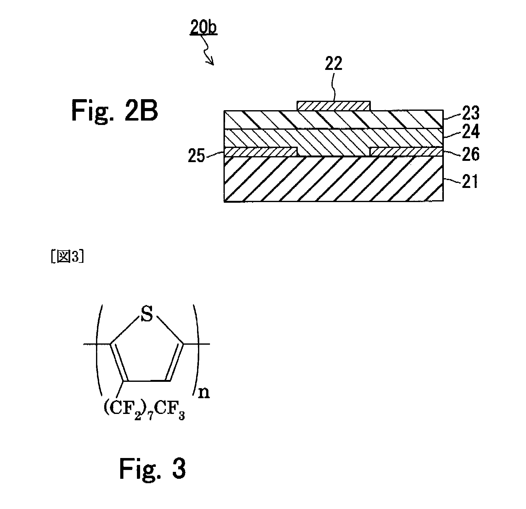
[0081] In Example 1, the description is directed to an example in which a polythiophene derivative (poly(3-perfluorooctylthiophene)) is used as the first organic molecules, while polystyrene is used as the second organic molecules.

(1) Method of Synthesizing Poly(3-Perfluorooctylthiophene)

[0082] The poly(3-perfluorooctylthiophene) shown in FIG. 3 was produced as follows. That is, 3-perfluorooctylthiophene was synthesized, and this was used as a starting material with which 2,5-dibromo-3-perfluorooctylthiophene was synthesized and then was polymerized. The methods of synthesizing 3-perfluorooctylthiophene, 2,5-dibromo-3-perfluorooctylthiophene, and poly(3-perfluorooctylthiophene) are described below sequentially.

(1-a) Method of Synthesizing 3-Perfluorooctylthiophene

[0083] In a mixed solution of copper powder 10 g, 3-iodothiophene 10.5 g, 3-perfluoro-n-octyliodide 32.8 g, and N,N-dimethylformamide 60 ml, a reaction was allowed to proceed in a dry nitrogen atmosphere at 120° C. fo...

example 2

[0106] In Example 2, the description is directed to an example in which a pentacene derivative (sulfinylperfluorooctaneamide-added pentacene) was used as the first organic molecules, while polystyrene was used as the second organic molecules. The sulfinylperfluorooctaneamide-added pentacene is a precursor of a semiconductor material.

(1) Method of Synthesizing Sulfinylperfluorooctaneamide-Added Pentacene

[0107] The sulfinylperfluorooctaneamide-added pentacene was synthesized by allowing pentacene and sulfinylperfluorooctaneamide to react each other. Sulfinylperfluorooctaneamide was synthesized from perfluorooctaneamide. The methods of synthesizing sulfinylperfluorooctaneamide and sulfinylperfluorooctaneamide-added pentacene are described below sequentially.

(1-a) Method of Synthesizing Sulfinylperfluorooctaneamide

[0108] First, perfluorooctaneamide (CF3(CF2)7CONH2) (46 g) was dissolved in n-hexane (300 ml). Thereafter, trimethylchlorosilane (15 ml) was dropped gradually into the s...

example 3

[0120] In Example 3, the description is directed to an example in which sulfinylperfluorooctaneamide-added pentacene that was described in Example 2 was used as the first organic molecules, while polyvinyl alcohol was used as the second organic molecules.

[0121] A coating liquid (C3) of Example 3 was prepared as follows. That is, sulfinylperfluorooctaneamide-added pentacene and polyvinyl alcohol were dissolved in a solvent so that the content of the former was 3 wt %, while the content of the latter also was 3 wt %. The solvent used herein was a mixed solvent of tetrahydrofuran and 2,2,2-trifluoroalcohol (whose volume ratio was 1:1). Thus an organic FET was produced by the same method as in Example 2 except that the coating liquid (C3) was used instead of the coating liquid (C2).

[0122] In addition, an organic FET of a comparative example was produced as follows. First, a chromium thin film and a gold thin film were formed on a quartz substrate. Next, a mixed solution of water and e...


PUM

PropertyMeasurementUnit
temperatureaaaaaaaaaa
weightsaaaaaaaaaa
weightsaaaaaaaaaa

Abstract

A method of manufacturing a field effect transistor of the present invention includes: applying a coating liquid 20 containing a solvent 13 as well as first and second organic molecules 11 and 12 that have been dissolved in the solvent 13; and forming a first layer and a second layer by removing the solvent 13 contained in the coating liquid 20 that has been applied. The first layer contains the first organic molecules 11 as its main component. The second layer adjoins the first layer and contains the second organic molecules 12 as its main component. The first organic molecules 11 are a semiconductor material or a precursor of a semiconductor material. The second organic molecules 12 are an insulator material or a precursor of an insulator material. The first organic molecules 11 and the second organic molecules 12 are not compatible with each other.

Description

TECHNICAL FIELD [0001] The present invention relates to a coating liquid for forming a layered film including an organic semiconductor layer and an organic insulating layer, a method of manufacturing a field effect transistor using the same, and a field effect transistor. BACKGROUND ART [0002] A field effect transistor (hereinafter also referred to as a “FET”) is an electronic device in which the value of current that flows between a source electrode and a drain electrode is controlled by voltage of a gate electrode. [0003] In this specification, a FET whose gate insulating layer and semiconductor layer each are formed of an organic material is referred to as an “organic field effect transistor” in some cases. In that FET, the semiconductor layer adjoins the gate insulating layer and functions as a channel region. A thin film made of an organic material can be formed on a substrate at around room temperature and also has mechanical flexibility. Accordingly, the organic FET can be fo...

Claims


Application Information

Patent Timeline
Patent Type & Authority Applications(United States)
IPC IPC(8): H01L31/00
CPCH01L51/0003H01L51/0007H01L51/0036H01L51/0545H01L51/052H01L51/0537H01L51/0541H01L51/0055H10K71/15H10K71/12H10K85/113H10K85/623H10K10/471H10K10/478H10K10/464H10K10/466
Inventor NAKAGAWA, TOHRU
Owner PANASONIC CORP
Why Eureka
Try Eureka