Two-layer film and method of forming pattern with the same
a two-layer film and resist technology, applied in the field of photofabrication, can solve the problems of difficult to observe the resist pattern with a light microscope, difficult to control the resist pattern profile in general, and failure of hdd, so as to improve the productivity of workpieces, confirm the undercut profile, and release easily
- Summary
- Abstract
- Description
- Claims
- Application Information
AI Technical Summary
Benefits of technology
Problems solved by technology
Method used
Image
Examples
examples
[0206] The present invention will be hereinafter described in detail by the following Examples, but it should be construed that the invention is in no way limited to those Examples Hereinafter, “parts” and “%” are by weight unless otherwise mentioned.
preparation examples
Preparation of Compositions 1 and 2
[0207] The following is a description of the components (A) to (H) that were used in the preparation of compositions (1-1) to (1-7) for lower layer production and compositions (2-1) to (2-2) for upper layer production.
(Synthesis of Radical Polymer A-1)
[0208] A flask equipped with a dry ice / methanol reflux condenser and a thermometer was purged with nitrogen. The flask was charged with a polymerization initiator: 3.0 g of 2,2′-azobisisobutyronitrile, and a solvent: 150 g of ethyl 2-hydroxypropionate. They were stirred together until the polymerization initiator dissolved in the solvent. Subsequently, 43 g of 4-isopropenylphenol (monomer I), 30.8 g of n-butyl acrylate (monomer III), 2.9 g of acrylic acid (monomer II) and 23.3 g of 2-hydroxyethyl crylate (monomer I) were introduced into the flask. The contents were stirred slowly to give a solution, which thereafter was heated to 70° C. Thus, polymerization was carried out at the temperature for 3 ...
example 1
Spin Coating / Spin Coating Process
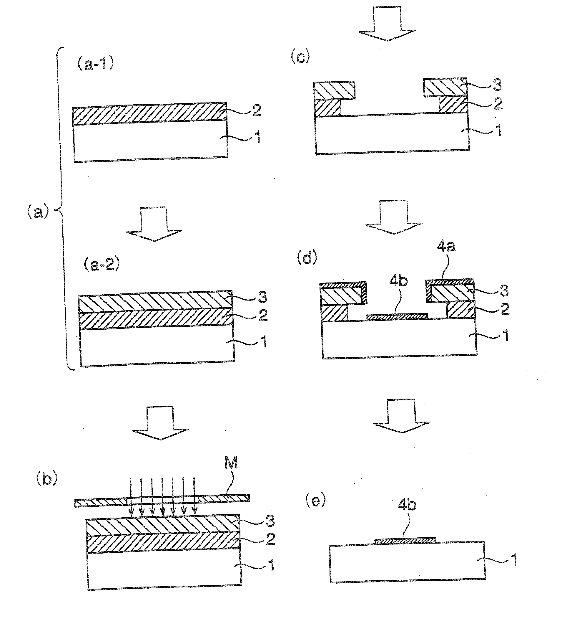
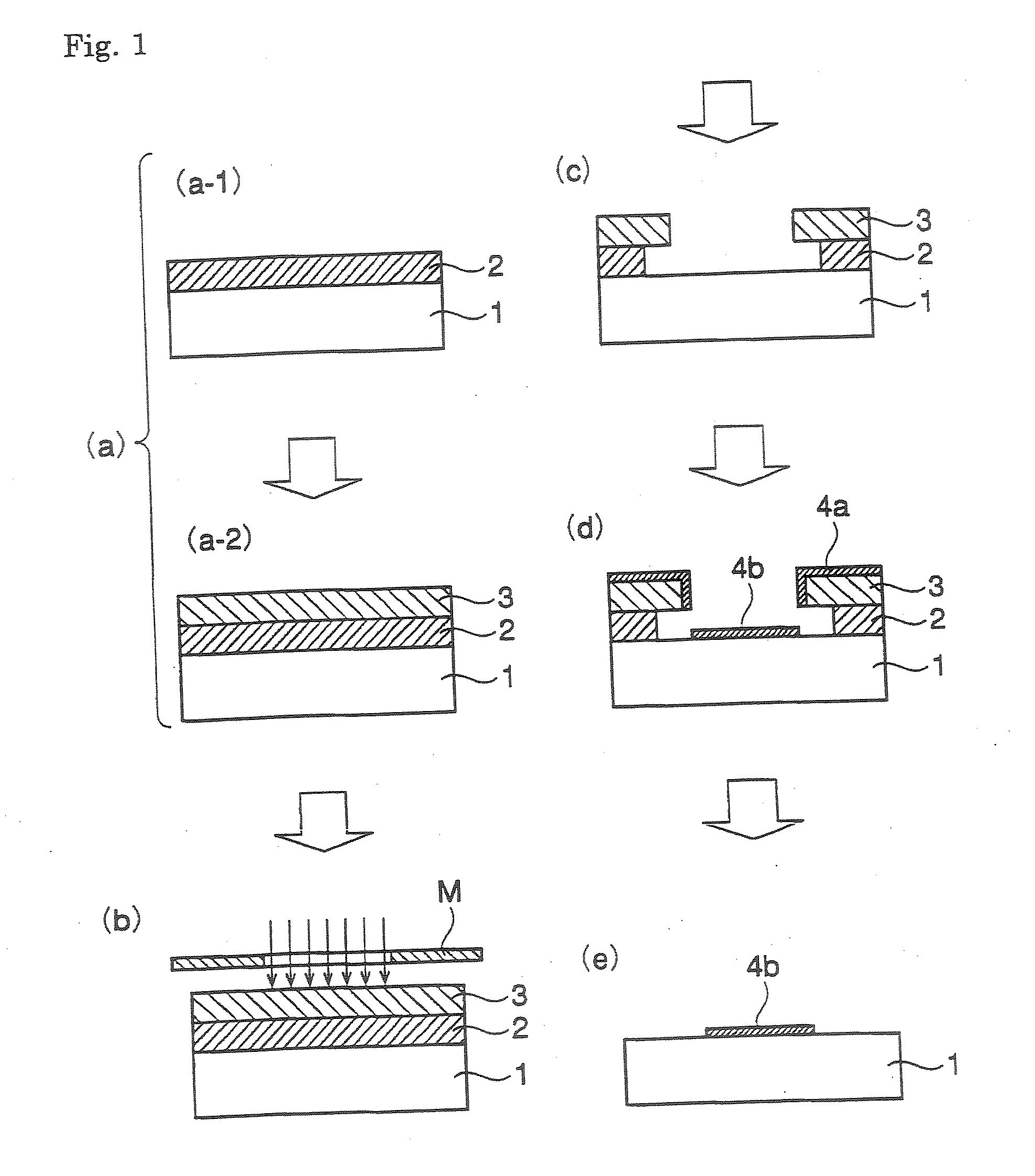
[0268] The composition (1-1) was dropped on a silicon wafer and spin coated thereon. The resultant coating was baked on a hot plate at 100° C. for 10 minutes to give a resist layer (I) (under layer) Thereafter, the composition (2-1) was dropped and spin coated on the above-formed under layer. The coating was baked on a hot plate at 100° C. for 5 minutes to give a resist layer (II) (upper layer). A two-layer laminate was thus obtained.
[0269] After the lower and upper layers had been formed on the substrate, the top surface of the laminate was observed with a light microscope. The surface condition was evaluated as either A or B based on the following criteria. The results are set forth in Table 3. [0270] Application properties A: the layers were uniform overall on the substrate [0271] B: the layers had released partially and had holes, i.e., the layers were not uniform overall on the substrate
[0272] The substrate having the layers evaluated above ...
PUM
| Property | Measurement | Unit |
|---|---|---|
| thickness | aaaaa | aaaaa |
| thickness | aaaaa | aaaaa |
| temperature | aaaaa | aaaaa |
Abstract
Description
Claims
Application Information


