Colored masking for forming transparent structures

a transparent structure and masking technology, applied in microlithography exposure apparatus, thin material processing, instruments, etc., can solve the problems of material extremly difficult to register, alignment errors, and use of very sophisticated and expensive equipment to ensure alignmen

Inactive Publication Date: 2007-11-22
EASTMAN KODAK CO
View PDF1 Cites 36 Cited by
  • Summary
  • Abstract
  • Description
  • Claims
  • Application Information

AI Technical Summary

Benefits of technology

[0006]The invention provides a method for forming aligned layers without the need for expensive alignment equipment and processes.

Problems solved by technology

For very precise operations employing rigid glass substrates, even small variations in temperature and humidity cause enough distortion of the existing or new patterns as to cause alignment errors.
This requires the use of very sophisticated and expensive equipment to ensure alignment.
Furthermore, when nonrigid supports are desired, the amount of dimensional variation with the materials make them extremely difficult to register.
Thus, a situation arises where for some applications, the most desirable and cheapest substrates cannot be used with the materials needed to make the desired devices.

Method used


Image

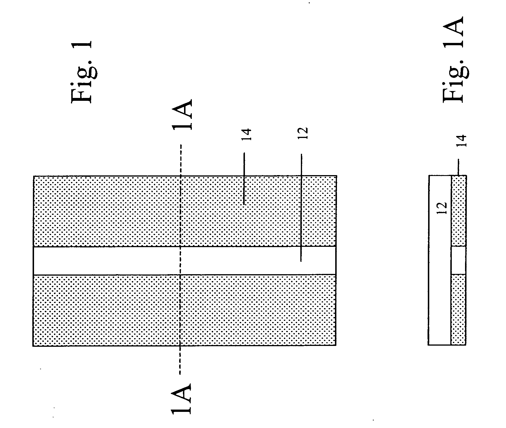
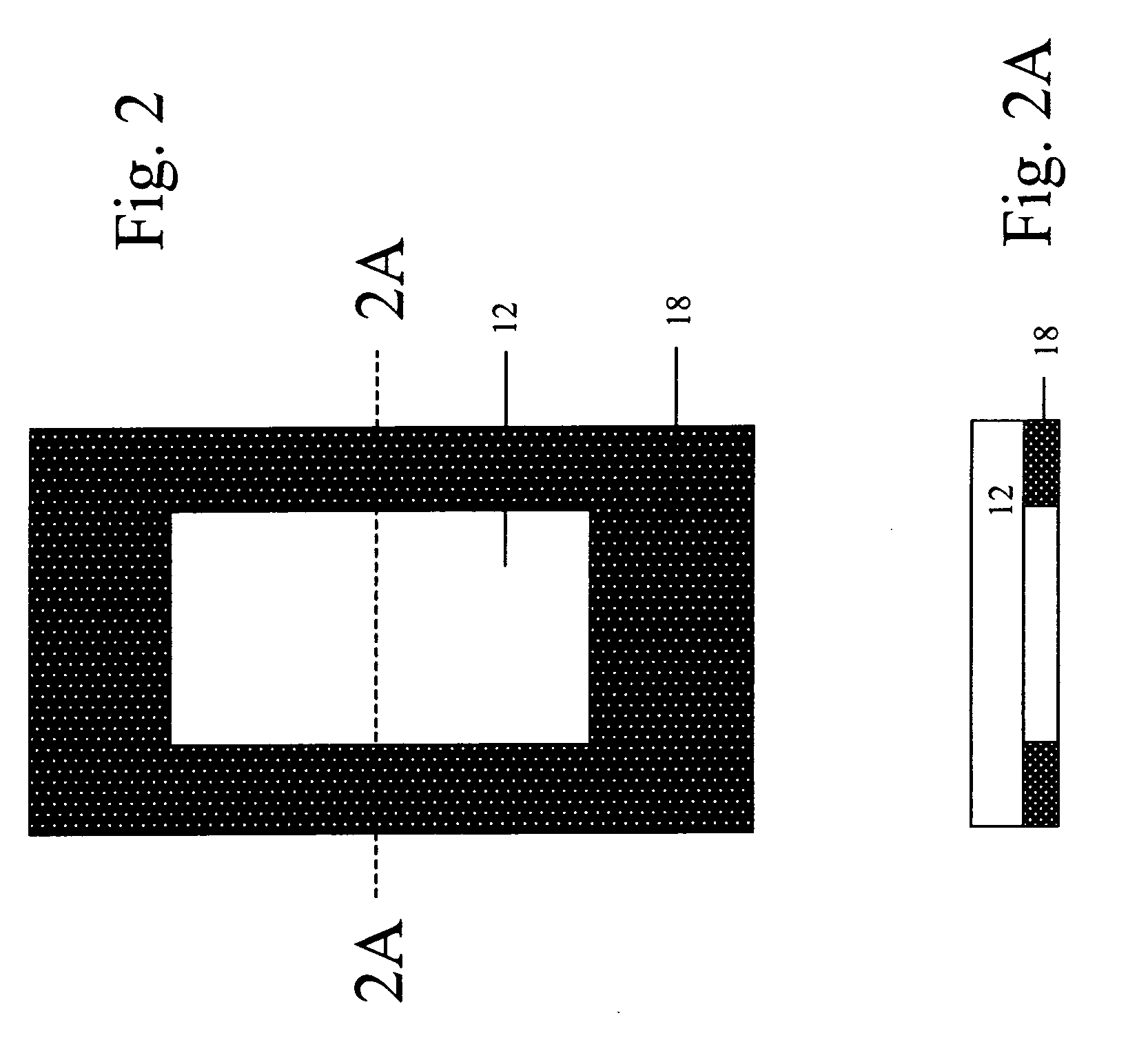
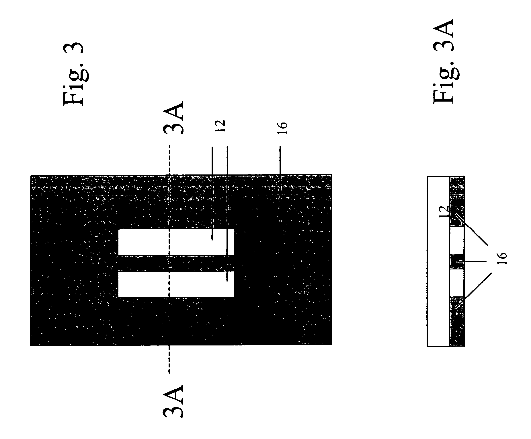
  • Colored masking for forming transparent structures
  • Colored masking for forming transparent structures
  • Colored masking for forming transparent structures

Examples


example 1

Multicolor Mask Formed by Direct Printing Process

[0114]In this example, a multicolor mask was prepared containing 3 color absorbing layers, with each color corresponding to an individual functional layer of an array of thin film transistor devices. The design for the gate layer of the array of thin film transistor devices was converted into a black and white bitmap file. The design for the semiconductor layer of the array of thin film transistor devices was converted into another black and white bitmap file. The design for the source and drain layer of the array of thin film transistor device was converted into a third black and white bitmap file. These bitmaps were then imported into the blue channel, green channel, and red channel of a single color image file using Photoshop 6.0. In this full color image, the blue channel contained the gate layer design as a yellow pattern. The green channel contained the semiconductor layer design as a magenta pattern. The red channel contained t...

example 2

Multicolor Mask Formed by Photolithography Process

[0115]In this example, a multicolor mask was prepared containing 3 color absorbing layers, with each color corresponding to an individual functional layer of an array of thin film transistor devices. Chrome on glass masks for the gate layer (CG-1), semiconductor and dielectric layers (CG-2), and source and drain layers (CG-3) of the array of thin film transistor devices were obtained from Applied Image Incorporated. A 0.7 mm thick borosilicate glass support was washed for 10 minutes by treating with a solution of 70% sulfuric acid and 30% of a 30% solution of hydrogen peroxide maintained at approximately 100 C. After washing, the clean glass was spin coated (at 1000 RPM) with Color Mosaic SC3200L (purchased from Fujifilm Electronic Materials Co., Ltd.). SC-3200L is a UV curable photoresist containing 3-5% of a cyan pigment, 7-9% of a methacrylate derivative copolymer, 7-9% of a polyfunctional acrylate resin and a UV photosensitizer d...

example 3

Blue-Curable Film Formulation

[0116]A coating solution C-1 for the blue light curable film was prepared as follows. A solution of blue sensitive photoinitiator was prepared by adding 0.03 g of photoinitiator A to 3 grams of toluene.

Photoinitiator A:

[0117]

[0118]In a separate vial, five grams of polymethylmethacrylate (PMMA) (MW ˜75K) were dissolved in 45 g of anisole. To 2.9 g of the resulting PMMA solution, 0.95 g of trimethylolpropane triacrylate and 0.5 g of the solution of photoinitiator A were added.

Green-Curable Film Formulation

[0119]A coating solution C-2 for the green light curable film was prepared as follows. A solution of green sensitive photoinitator was prepared by adding 0.03 g of photoinitiator B to 3 grams of anisole. In a separate vial, five grams of PMMA (MW ˜75K) were dissolved in 45 g of anisole. To 2.9 g of the resulting PMMA solution, 0.95 g of trimethylolpropane triacrylate and 0.5 g of the solution of photoinitiator B were added.

Photoinitiator B:

[0120]


PUM

PropertyMeasurementUnit
absorption wavelengthaaaaaaaaaa
optical densityaaaaaaaaaa
diameteraaaaaaaaaa

Abstract

The invention relates to a process for forming a stacked transparent structure comprising providing a support, coating one side of said support with a multicolored mask, coating the other side of the support with a layer curable by visible light, and exposing the light-curable layer through the mask with visible light to cure the layer curable by light in exposed portions to form a cured pattern.

Description

FIELD OF THE INVENTION[0001]The invention relates to a colored masking technique useful for forming electrical components.BACKGROUND OF THE INVENTION[0002]There exist a number of technologies which rely upon accurately patterned sequential layers of electrically and optically active materials applied to a relatively large substrate. Well known applications that might require this include the manufacture of electronic components, flat panel displays, radio frequency identification (RFID) tags, and various sensing applications.[0003]The reasons for patterning accuracy are twofold. First of all, patterned features must be reproduced across large areas of a substrate while having precise control over their dimensions. Secondly, products built with these features typically are composed of several layers of different, but interacting patterned layers, where it is important that the layers be in specific registration. In current practice, the registration is typically achieved using sophis...

Claims


Application Information

Patent Timeline
Patent Type & Authority Applications(United States)
IPC IPC(8): G03F7/20
CPCG03F1/14G03F1/56Y10T428/24802G03F7/2018Y10T428/24917G03F7/2014G03F7/0035G03F7/027
Inventor IRVING, LYN M.LEVY, DAVID H.IRVING, MARK E.
Owner EASTMAN KODAK CO
Why Eureka
Try Eureka