Polymer compound and organic light-emitting device using the same
a technology of organic light-emitting devices and polymer compounds, which is applied in the direction of organic conductors, non-metal conductors, conductors, etc., can solve the problems of low quantum efficiency, color purity, thermostability, etc., and achieve the effect of reducing the number of oleds
- Summary
- Abstract
- Description
- Claims
- Application Information
AI Technical Summary
Benefits of technology
Problems solved by technology
Method used
Image
Examples
synthesis examples
Synthesis of Phenoxazine Monomer
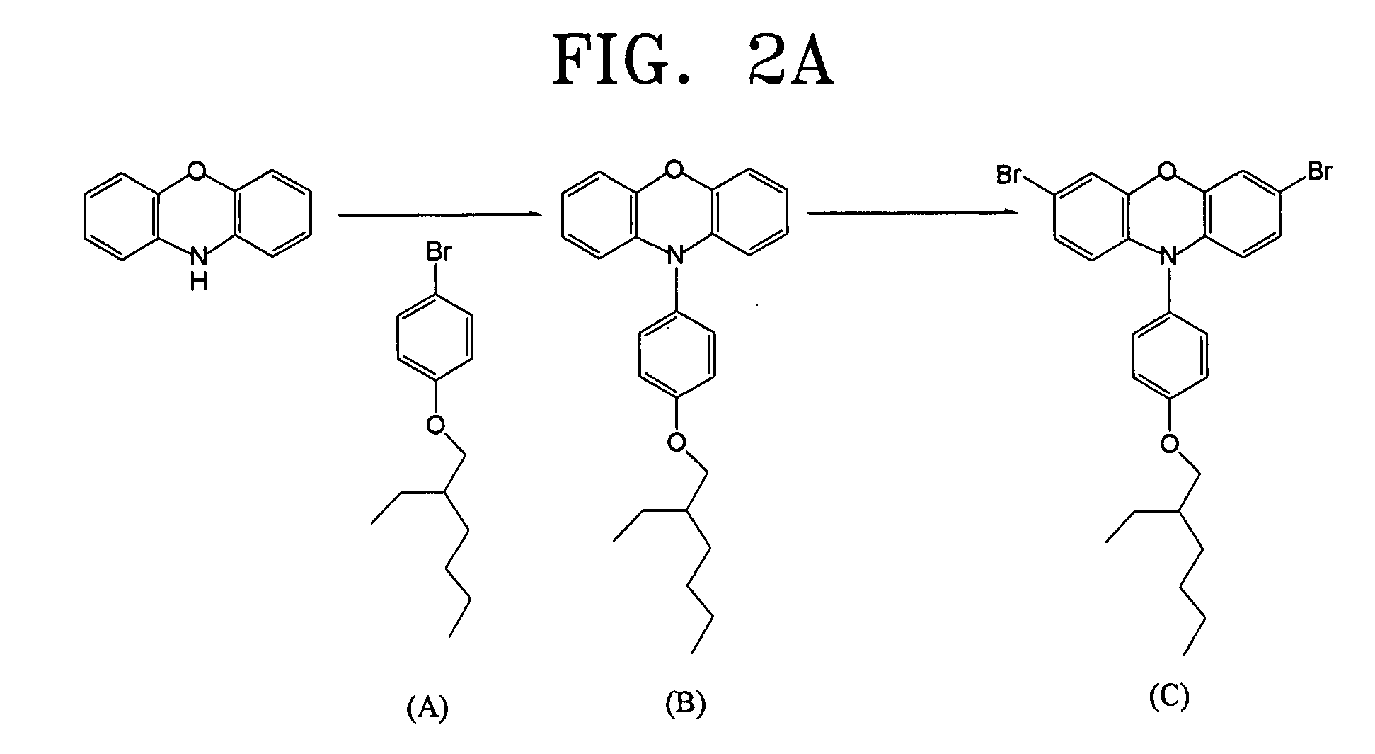
[0057]1) Preparation of Compound (A)
[0058]50 g (0.29 mole) of 4-bromophenol was dissolved in 500 ml of acetone, and 48.4 g (0.35 mole) of K2CO3 was added thereto. Then, 73.3 g (0.38 mole) of 1-bromooctane was added to the mixture and the mixture was refluxed for 24 hours.
[0059]After the reaction was ended, an organic layer was extracted using a solution of water:CHCl3=2:1 (volume-ratio), and K2CO3 is removed. The organic layer was dried with MgSO4, condensed, and applied to silica-gel column chromatography using hexane as an eluent. The unreactant 1-bromooctane was removed from the resulting eluate, using distillation under reduced pressure, thereby resulting in 80 g of compound (A) (yield: 96%) The structure of compound (A) was identified using 1H-NMR.
[0060]2) Preparation of Compound (B)
[0061]18 g (64 mmol) of compound (A), 10 g (54 mmol) of phenoxazine, 7.4 g (77 mmol) of sodium tert-butoxide, 0.61 g (1.1 mmol) of (Tris(dibenzylidene acetone)dipalla...
example 1
[0077]
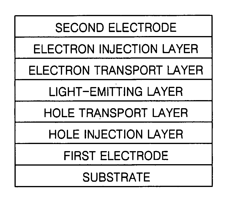
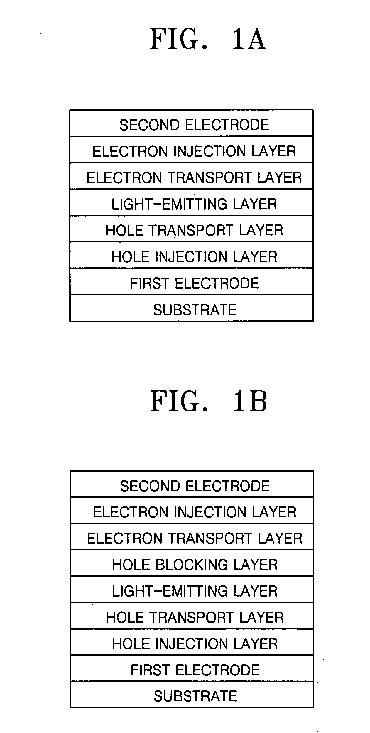
[0078]First, a transparent electrode substrate was prepared by coating indium-tin oxide (ITO) on a glass substrate and washing the substrate. Then ITO was patterned using photoresist resin and etchant to desired patterns and the substrate washed. A hole injection layer was formed by coating the compound of Formula 2 on the substrate using a solution process where toluene was used as a solvent, to a thickness of about 50 nm, and baking at 110° C. for about one hour. Then, an emissive layer forming material was prepared by dissolving 0.8 weight % of the polymer of Formula 9 in 99.2 weight % of m-xylene. The polymer solution was filtered with 0.45 μm filter, and the material was spin-coated on the hole injection layer, baked, and removed completely of solvent in vacuum oven to form a polymer thin layer. The thickness of the polymer thin layer was controlled to about 80 nm by controlling the concentration and the spin-speed of the polymer solution. Then, 2.7 nm of a Ca layer and a...
example 2
[0080]An organic EL device was manufactured using the process of Example 1 except that 5 weight % of tetrafluorotetracyanoquinonedimethane (F4TCNQ) relative to the weight of the host was co-injected as a dopant with the compound of Formula 2 to form a hole injection layer.
[0081]The turn-on voltage of the device was 3.5V, the light-emitting efficiency was 4.6 cd / A, and the color coordinates were (0.16, 0.28).
PUM
| Property | Measurement | Unit |
|---|---|---|
| temperature | aaaaa | aaaaa |
| melting point | aaaaa | aaaaa |
| melting point | aaaaa | aaaaa |
Abstract
Description
Claims
Application Information


