Modifying the optical properties of a nitride optoelectronic device

a technology of optoelectronic devices and nitride, which is applied in the direction of lasers, semiconductor devices, semiconductor lasers, etc., can solve the problems of low deposition rate, prone to catastrophic optical damage of the cleaved facets of the semiconductor laser device, and lack of precise control of the thickness or composition of the deposited overgrowth layer, etc., to achieve novel and improved optical characteristics and performance of the device, and the thickness and composition of the or each nitrid

Inactive Publication Date: 2008-01-17
SHARP KK
View PDF24 Cites 13 Cited by
  • Summary
  • Abstract
  • Description
  • Claims
  • Application Information

AI Technical Summary

Benefits of technology

[0023] A method of the invention uses a growth method such as, for example, plasma-assisted MBE to grow the one or more nitride semiconductor layers over the nitride semiconductor light-emitting device. This allows much more precise control of the thickness and composition of the or each nitride semiconductor layer. The method of the invention also allows the nitride semiconductor layer(s) to be grown

Problems solved by technology

As one example, the cleaved facets of a semiconductor laser device are prone to suffer catastrophic optical damage (“COD”) as a result of heat generation at the air-facet interface leading to localised heating of the facet and degradation of the laser diode's light-emitting regi

Method used


Image

  • Modifying the optical properties of a nitride optoelectronic device
  • Modifying the optical properties of a nitride optoelectronic device
  • Modifying the optical properties of a nitride optoelectronic device

Examples


Embodiment Construction

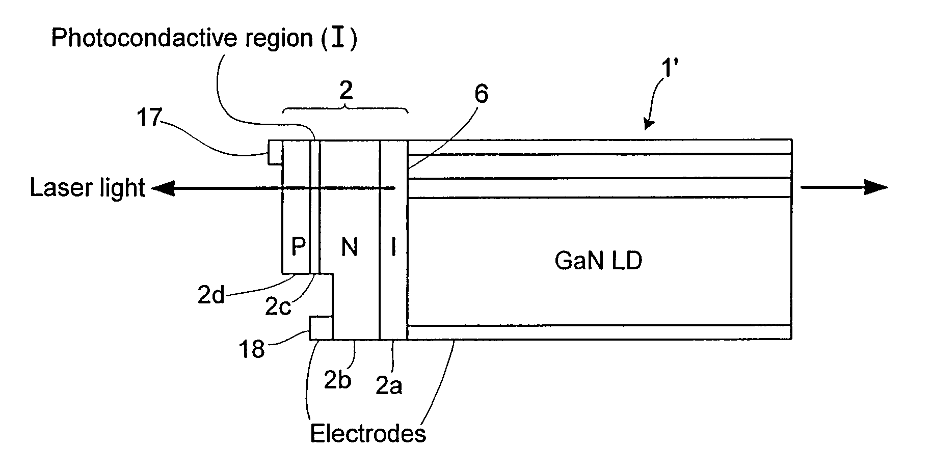
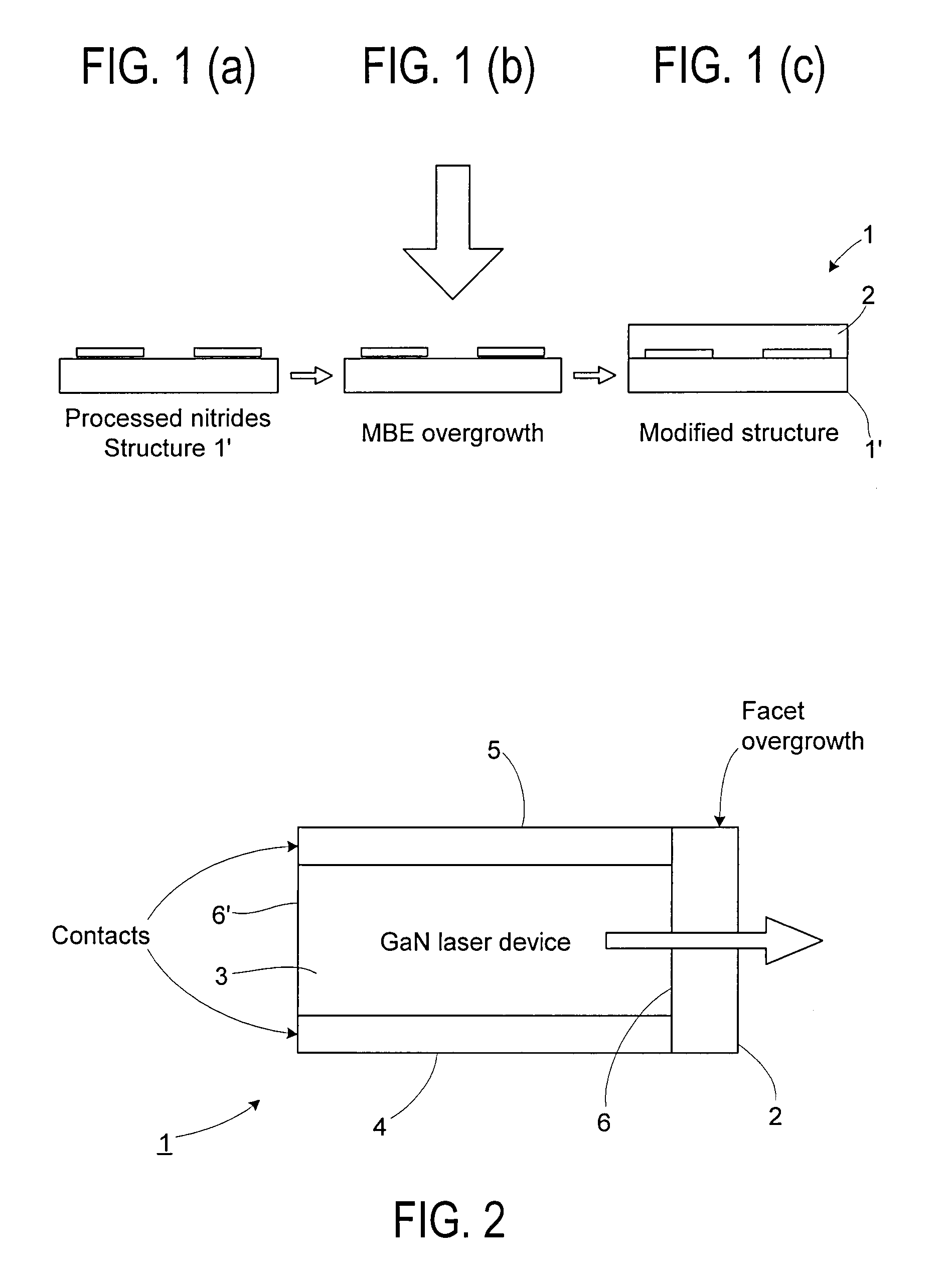
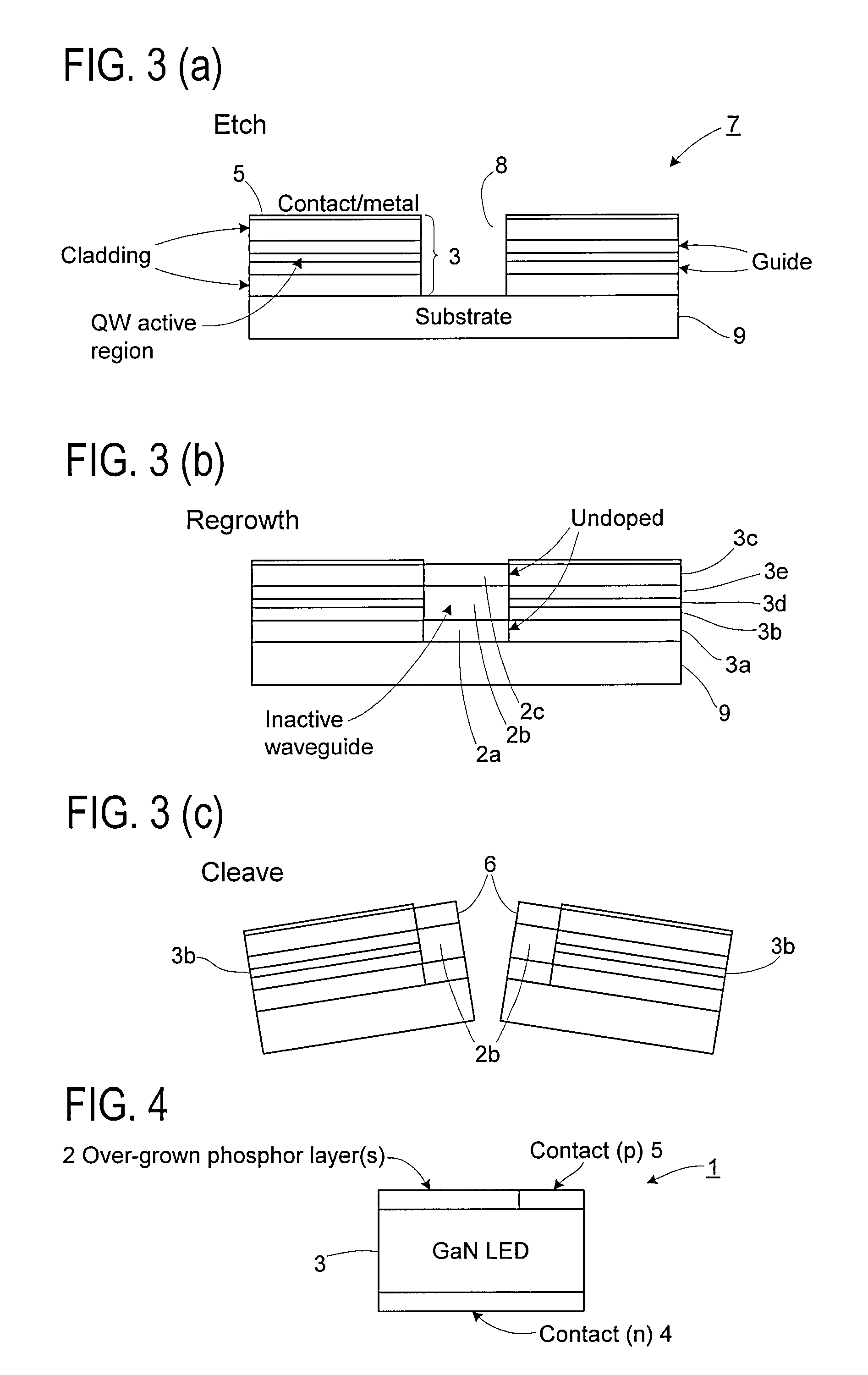
[0057] According to the present invention a plasma-assisted growth method, such as, for example, plasma-assisted MBE, is used to grow one or more nitride semiconductor layers over a processed semiconductor optoelectronic device, in order to modify its optical emission properties. FIG. 1(a) to FIG. 1(c) illustrate the principal stages of a method of the present invention.

[0058] The invention takes as its starting point a nitride semiconductor light-emitting device structure 1′ that has been processed in some way. The light-emitting device structure 1′ may have been grown according to any conventional semiconductor growth technique such as metal organic chemical vapour deposition (MOCVD) or molecular beam epitaxy. A processed semiconductor optoelectronic device is defined as a structure that has been converted from its “as-grown form” by one or more of: dicing, cleaving, etching, annealing, deposition, patterning, implantation or oxidation.

[0059] A processed nitride optoelectronic d...


PUM


Abstract

A method of modifying the optical properties of a processed nitride semiconductor light-emitting device initially comprises disposing the processed nitride semiconductor light-emitting device in a vacuum chamber. One or more nitride semiconductor layers are then grown by molecular beam epitaxy thereby to modify the optical properties of the processed light-emitting device. Activated nitrogen, for example from a plasma source, is supplied to the vacuum chamber during growth of the nitride semiconductor layer(s). The use of activated nitrogen reduces the growth temperature required for the growth of the nitride semiconductor layer(s), as the need for thermal activation of a nitrogen species is eliminated. Moreover, use of a growth method such as, for example, plasma-assisted MBE to grow the nitride semiconductor layer(s) allows much more precise control of their thickness and composition.

Description

[0001] This Nonprovisional application claims priority under 35 U.S.C. § 119(a) on British Patent Application No. 0613890.3 filed in U.K. on 13 Jul. 2006, the entire contents of which are hereby incorporated by reference. FIELD OF THE INVENTION [0002] The present invention relates to a method of modifying the optical properties of a nitride optoelectronic device such as, for example, a nitrides laser diode or a nitrides light-emitting diode. It particularly relates to a method in which one or more nitride semiconductor layers are grown over the nitride optoelectronic device so as to modify the optical emission properties of the device. BACKGROUND OF THE INVENTION [0003] Fabrication of an optoelectronics device in a nitride semiconductor system, such as the (Al,Ga,In)N materials system for example, is well-known. In summary, a semiconductor layer structure in the form of a “wafer” is grown in a suitable growth apparatus. The as-grown wafer has a typical diameter of 5 cm. After remova...

Claims


Application Information

Patent Timeline
IPC IPC(8): H01L33/00
CPCH01L33/007H01S5/005H01S5/0202H01S2304/12H01S5/0282H01S2304/02H01S5/028H01S5/0264H01S5/0281
Inventor HOOPER, STEWART EDWARDKAUER, MATTHIASHEFFERNAN, JONATHANALDERMAN, JOANNA CATHERINEBARNES, JENNIFER MARYBOUSQUET, VALERIEKAMIKAWA, TAKESHITAKAHIRA, YOSHIYUKI
Owner SHARP KK
Why Eureka
Try Eureka