Semiconductor manufacturing system

a manufacturing system and semiconductor technology, applied in the direction of coatings, metallic material coating processes, chemical vapor deposition coatings, etc., can solve the problems of long film-forming time, short life of ozone under elevated temperature conditions, and difficult uniform formation of dielectric films by cvd in high aspect ratio grooves with high coverage, etc., to achieve the effect of preventing the generation of particles

Inactive Publication Date: 2008-03-20
TOKYO ELECTRON LTD
View PDF0 Cites 9 Cited by
  • Summary
  • Abstract
  • Description
  • Claims
  • Application Information

AI Technical Summary

Benefits of technology

[0019] In the most typical embodiment of the present invention described later with reference to the accompanying drawings, the first film-forming gas is ozone; the second film-forming gas is TEMAH gas; the third film-forming gas is trimethyl aluminum (hereinafter abbreviated as “TMA”) gas; the first precoating gas is ozone; and the second precoating gas is TMA gas. Further, the semiconductor manufacturing system is a vertical, batch-type system that accommodates a plurality of semiconductor substrates arrayed vertically in horizontal posture in the reaction vessel, and performs a film-forming process to the semiconductor substrates collectively. Further, the film-forming nozzle for supplying the first film-forming gas (i.e., ozone) is a distributing nozzle having a plurality of nozzle holes for discharging the first film-forming gas toward the plurality of semiconductor substrates from thei

Problems solved by technology

However, it is difficult by CVD to uniformly form a dielectric film in a high aspect ratio groove with a high coverage.
ALD is advantageous in its excellent film-thickness reproducibility, but is disadvantageous in its long film-forming time.
On the other hand, ozone has a short life under elevated temperature conditions.
However, the supply of an excessive amount of ozone causes oxidation damage to the components in the lower portion of the reaction chamber 1101, which is not desirable.
Furthermore, ozone is consumed by this oxidation reaction.
Incidentally, particle reduction is a critical issue in semiconductor manufacturing.
When a film is formed on the semiconductor substrates by CVD, ALD, or other chemical deposition process, deposition of unnecessary films unavoidably occurs on the inner wall of the reaction tube and on the various components that are exposed to the atmosphere within the reaction vessel.
Peeling-o

Method used


Image

  • Semiconductor manufacturing system
  • Semiconductor manufacturing system
  • Semiconductor manufacturing system

Examples


Embodiment Construction

[0034] The present invention will be described in detail with reference to the results of studies and experiments conducted by the present inventors to achieve the invention.

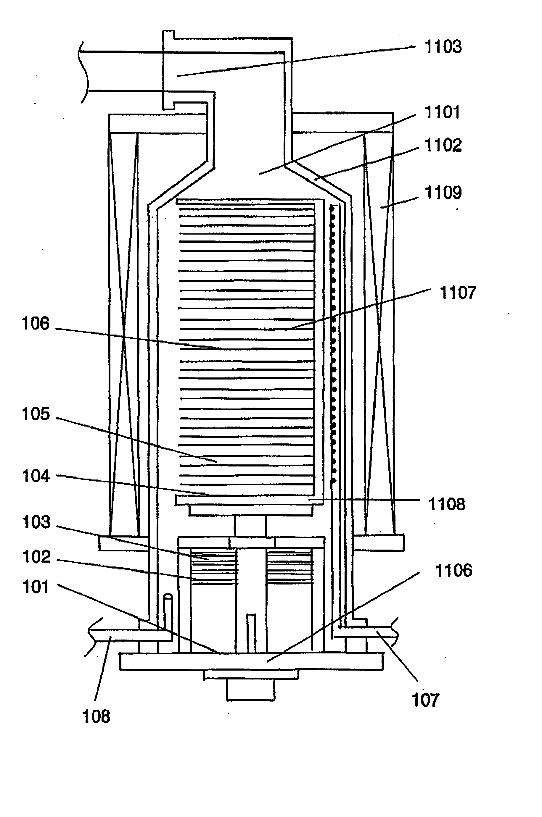
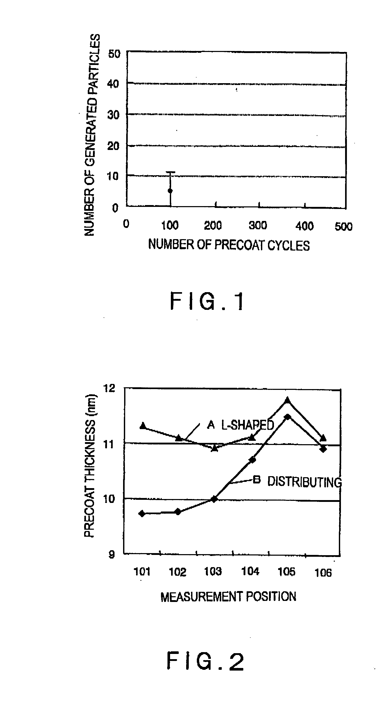
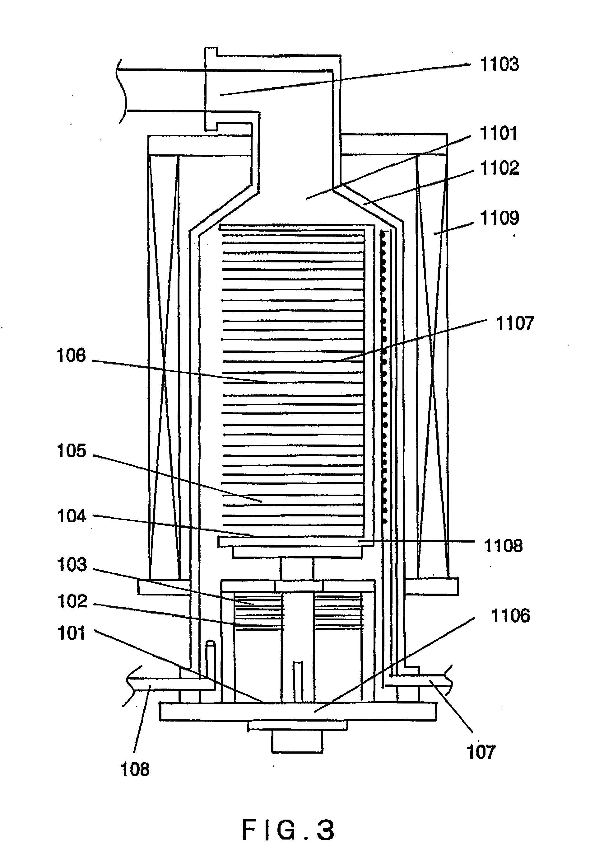
[0035] A precoating technique has been used to prevent the generation of particles resulting from peeling-off of unnecessary films in CVD apparatus. The precoating technique coats potentially peelable unnecessary films with a film (e.g., an SiO2 film) to prevent peeling-off of the unnecessary films. The present inventors have tried to extend this technique.

[0036] The present inventors conducted an experiment in which an HfO film was coated with an aluminum oxide (hereinafter referred to as an “AlO”) film. The AlO film was formed by an ALD process that repeats, a plurality of times, a deposition cycle consisting of a TMA gas flowing step, an evacuating step, a nitrogen gas flowing (purging) step, an ozone flowing step, an evacuating step, and a nitrogen gas flowing (purging) step which were performed in that or...


PUM


Abstract

Disclosed is a technique for effectively suppressing the generation of particles resulting from peeling-off of unnecessary films that have unavoidably adhered to the inner surface of the reaction tube of an ALD film-forming apparatus. A precoating process utilizing ALD is performed to deposit a metal oxide film, e.g., an aluminum oxide film, onto the unnecessary films, in order to prevent peeling-off of the unnecessary films. The type and/or position of the nozzle for supplying ozone, as a precoat gas, into the reaction tube during the precoating process is different from that of the nozzle for supplying ozone, as a film-forming gas, into the reaction tube during forming of a film on a semiconductor substrate.

Description

TECHNICAL FIELD [0001] The present invention relates to semiconductor manufacturing system and particularly to coating apparatus for forming a film of a desired thickness by repeating atomic or molecular level deposition. More particularly, the Invention relates to a technique of effectively precoating the inside of the reaction vessel to prevent the generation of particles. BACKGROUND ART [0002] With higher integration of semiconductor devices, the miniaturization of their device pattern progresses. For example, 1-gigabit dynamic random access memory (DRAM) has been used in practical applications. Such large capacity DRAM employs elements reduced in dimension and hence in surface area. Since DRAM uses the amount of charge stored on its memory cell capacitors as stored information, these capacitors must have a capacitance greater than a certain value. Therefore, memory cell capacitors currently have a very high aspect ratio. Conventionally, CVD (Chemical Vapor Deposition) is used to...

Claims


Application Information

Patent Timeline
IPC IPC(8): C23C16/00
CPCC23C16/45548C23C16/405H01L21/31
Inventor MOROZUMI, YUICHIROKOYANAGI, KENICHIARAO, TAKASHIUNE, KAZUNORI
Owner TOKYO ELECTRON LTD
Why Eureka
Try Eureka