Nitride semiconductor device and method for fabricating the same

a semiconductor and semiconductor technology, applied in the field of nitride semiconductor devices, can solve the problems of difficult for the fet to exhibit enhancement-type (normally off-type) characteristics, and achieve the effect of preventing current collapse, small on-resistance and preventing current collaps

Active Publication Date: 2008-04-03
PANASONIC CORP
View PDF14 Cites 73 Cited by
  • Summary
  • Abstract
  • Description
  • Claims
  • Application Information

AI Technical Summary

Benefits of technology

[0014]In view of the conventional problem described above, an object of the present invention is to provide a solution capable of preventing current collapse caused in normally-off type nitride semiconductor devices applicable to power transistors.
[0017]With the nitride semiconductor device according to the present invention, the p-type third nitride semiconductor layer formed on the second nitride semiconductor layer having a larger band gap energy than the first nitride semiconductor layer has a thickness greater in a portion below the gate electrode than in a portion below the side of the gate electrode. Thereby, the electron gas concentration in two-dimensional electron gas generated around the interface of the first nitride semiconductor layer with the second nitride semiconductor layer becomes lower in the region immediately below the gate electrode than in the region below the side of the gate electrode, so that the threshold voltage can be shifted to a positive direction. Moreover, in a portion of the first nitride semiconductor layer located below the side of the gate electrode, the two-dimensional electron gas concentration is higher than that in the case where the third nitride semiconductor layer is not provided. That is to say, if the third nitride semiconductor layer is not provided on the second nitride semiconductor layer, a surface state appears on the surface of the second nitride semiconductor layer, and electrons trapped by the appearing surface state has some influences such as a change of the two-dimensional electron gas to a depletion state. On the other hand, if the third nitride semiconductor layer is provided on the second nitride semiconductor layer like the present invention, the influences such as a change of the two-dimensional electron gas to a depletion state are decreased, so that the current collapse can be prevented.
[0032]With the first method for fabricating a nitride semiconductor device, the p-type third and fourth nitride semiconductor layers are formed on the second nitride semiconductor layer having a larger band gap energy than the first nitride semiconductor layer, and by the p-type third and fourth nitride semiconductor layers, the electron gas concentration in two-dimensional electron gas generated around the interface of the first nitride semiconductor layer with the second nitride semiconductor layer can be lower in a portion of the first nitride semiconductor layer located below the gate electrode than in the gate electrode region, so that the threshold voltage can be shifted to a positive direction. Moreover, in a portion of the first nitride semiconductor layer located below the side of the gate electrode, the two-dimensional electron gas concentration is higher than that in the case where the third nitride semiconductor layer is not provided, which increases the absolute value of the negative threshold voltage of a virtual transistor element provided as a virtual component and formed through a surface depletion layer. Thereby, the influence of the surface state on the two-dimensional electron gas generated in the area below the side of the gate electrode can be reduced, and thus the current collapse can be prevented.
[0036]With the second method for fabricating a nitride semiconductor device according to the present invention, the p-type third nitride semiconductor layer is formed on the second nitride semiconductor layer having a larger band gap energy than the first nitride semiconductor layer, and by the p-type third nitride semiconductor layer, the electron gas concentration in two-dimensional electron gas generated around the interface of the first nitride semiconductor layer with the second nitride semiconductor layer can be lower in a portion of the first nitride semiconductor layer located below the gate electrode than in the portion thereof below the side of the gate electrode, so that the threshold voltage can be shifted to a positive direction. Moreover, in a portion of the first nitride semiconductor layer located below the side of the gate electrode, the two-dimensional electron gas concentration is higher than that in the case where the third nitride semiconductor layer is not provided, whereby the current collapse can be prevented.
[0037]As described above, with the nitride semiconductor device and its fabrication method according to the present invention, a normally-off type nitride semiconductor device having a small on-resistance and preventing the current collapse can be provided.

Problems solved by technology

As a result of this, in the case where a FET is fabricated from this material, the fabricated FET is likely to exhibit depletion type (normally-on type) characteristics, and hence it is difficult for the FET to exhibit enhancement-type (normally-off type) characteristics.
Since the occurrence of the current collapse significantly increases the on-resistance, this becomes an extremely serious problem for a power transistor to which a high drain voltage is applied.

Method used


Image

  • Nitride semiconductor device and method for fabricating the same
  • Nitride semiconductor device and method for fabricating the same
  • Nitride semiconductor device and method for fabricating the same

Examples


first embodiment

[0050]A first embodiment of the present invention will be described with reference to the accompanying drawings.

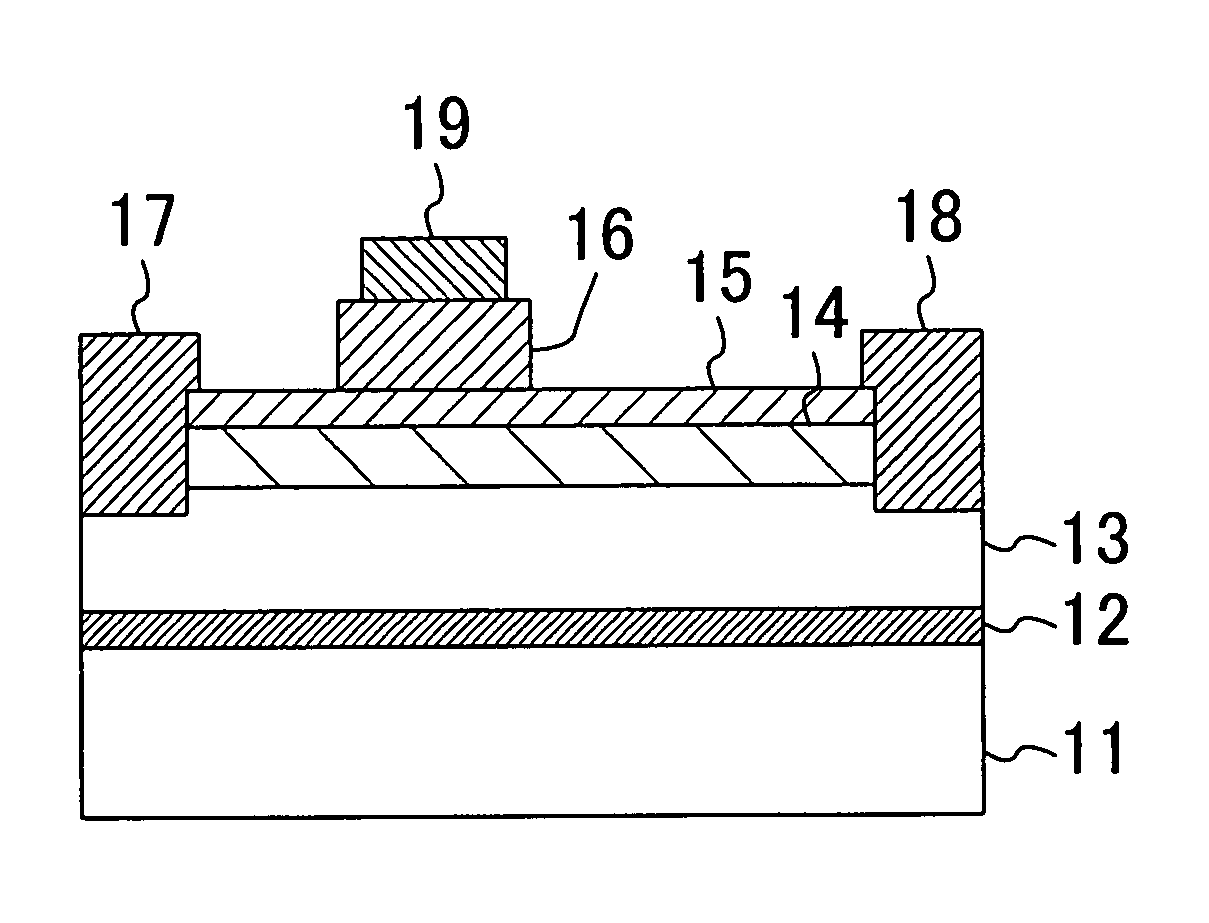
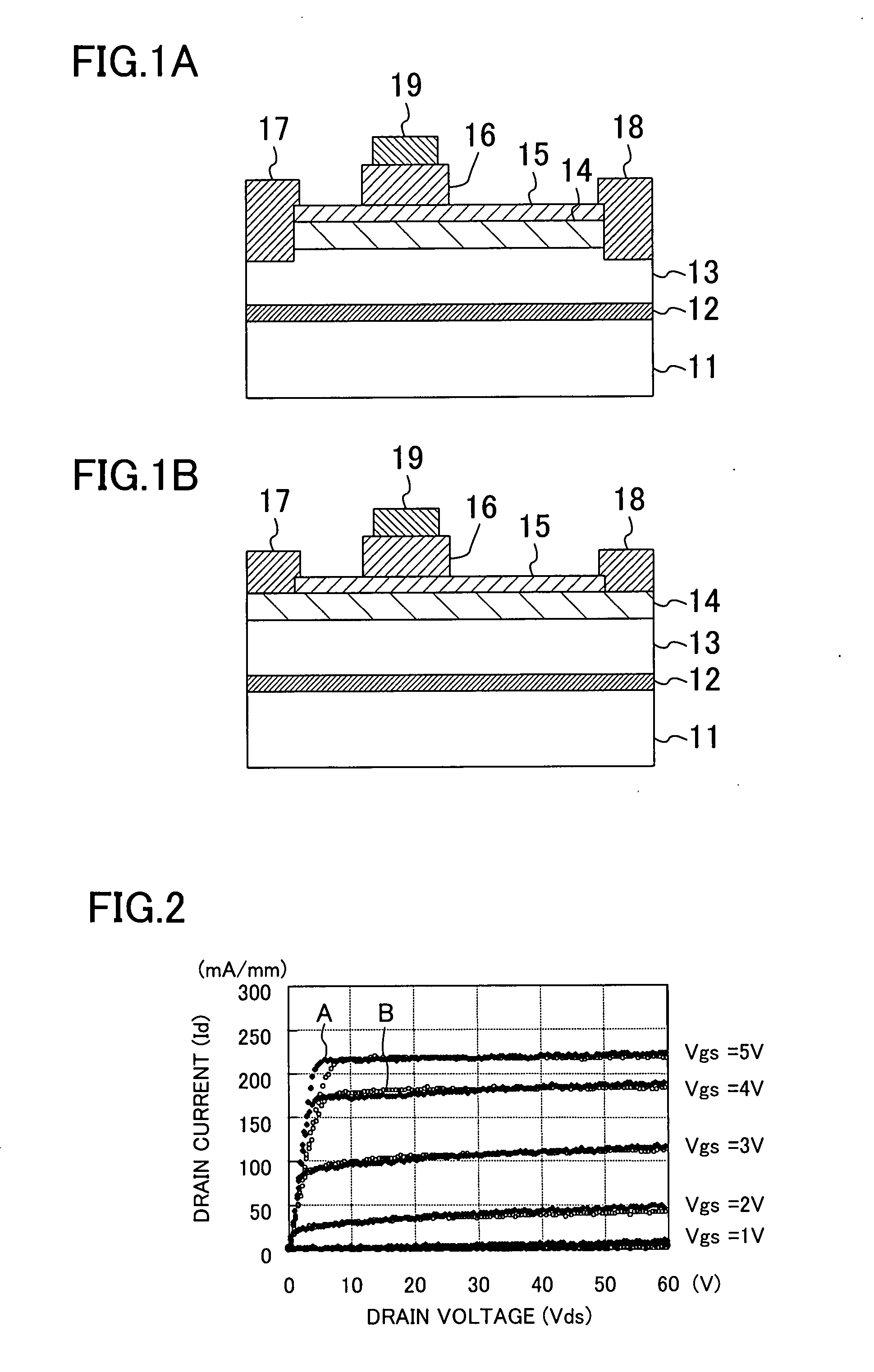
[0051]FIG. 1A shows a cross-sectional structure of a nitride semiconductor device (JFET) according to the first embodiment of the present invention. Referring to FIG. 1A, the nitride semiconductor device according to the first embodiment has a substrate 11, a buffer layer 12, a channel layer 13, a barrier layer 14, a p-type AlGaN layer 15, and a p-type GaN layer 16. The substrate 11 is made of sapphire and the orientation of the principal plane thereof is the (0001) plane. The buffer layer 12 of aluminum nitride (AlN) is formed on the principal plane of the substrate 11 and has a thickness of 100 nm. The channel layer 13 of undoped gallium nitride (GaN) is provided on the buffer layer 12 and has a thickness of 2 μm. The barrier layer 14 of undoped aluminum gallium nitride (AlGaN) is formed on the channel layer 13 and has a thickness of 25 μm. The p-type AlGaN layer 15 as a...

second modification

of First Embodiment

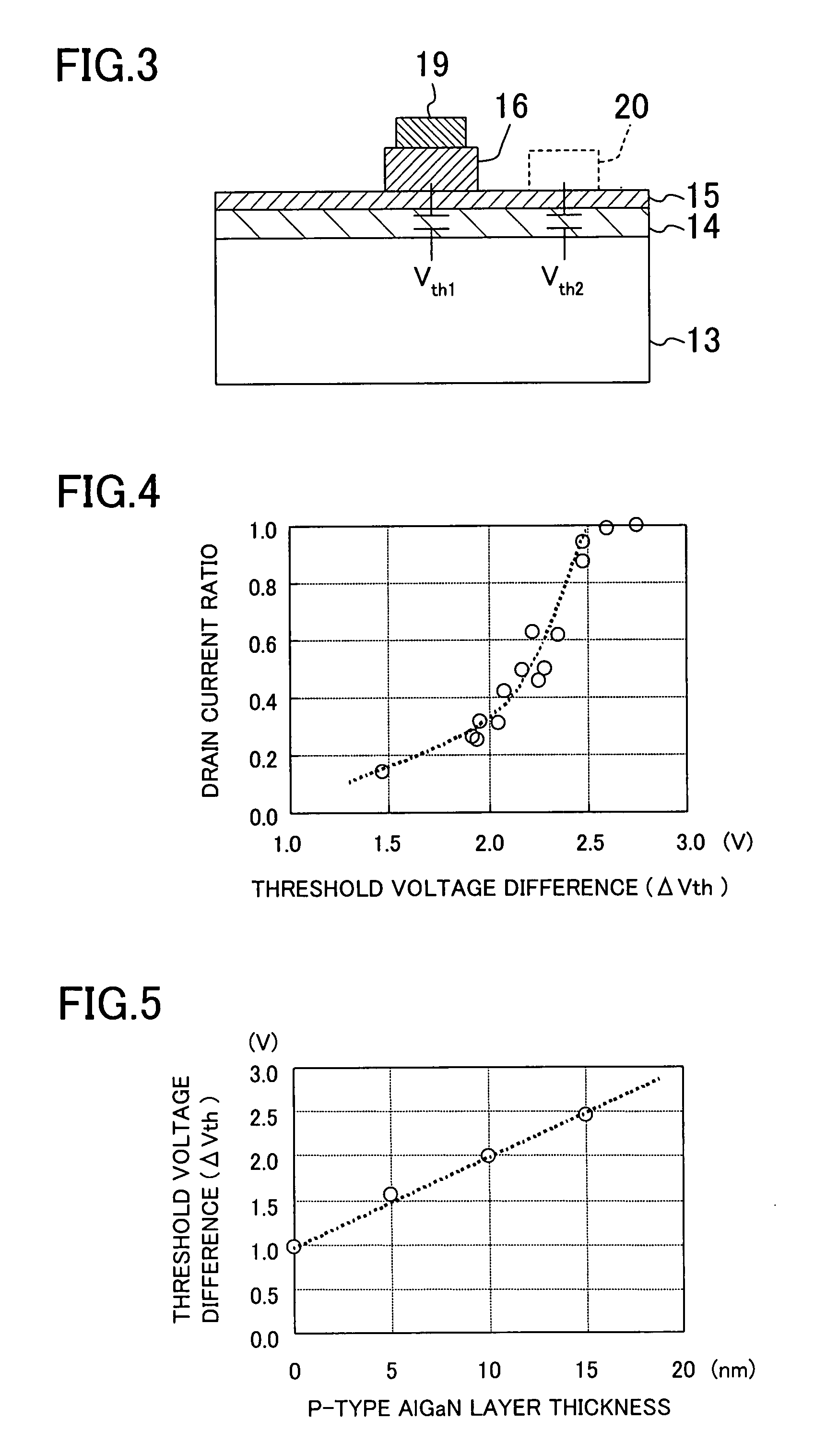
[0081]In the first embodiment, as shown in FIG. 1, in the p-type AlGaN layer 15 provided on the barrier layer 14, the thickness below the gate electrode 19 and the thickness below the side of the gate electrode 19 are substantially identical.

[0082]However, as in the case of a second modification shown in FIG. 7, in the p-type AlGaN layer 15, the thickness below the side of the gate electrode 19 may be made smaller than the thickness below the gate electrode 19 so that the thickness below the gate electrode 19 is set at about 20 nm and the thickness below the side of the gate electrode 19 is set at about 15 nm.

[0083]With this structure, the nitride semiconductor device according to the second modification can prevent the current collapse like the first embodiment. In addition to this, a corner provided at the side of the gate electrode 19 and having a maximum electric field intensity in applying a high drain voltage is formed only of the p-type AlGaN layer 15 with ...

third modification

of First Embodiment

[0084]Not only the nitride semiconductor device has the structure in which the p-type GaN layer 16 is formed only below the gate electrode 19, but also it may have a structure in which, like a nitride semiconductor device according to the third modification shown in FIG. 8, part of the p-type GaN layer 16 is also formed below the side of the gate electrode 19. In this structure, if an exposed portion of the p-type GaN layer 16 formed below the side of the gate electrode 19 is thick, it will cause an increase in a leakage current flowing between the gate and the drain or between the gate and the source. Thus, the exposed portion desirably has a thickness of about 20 nm or less. This makes it possible to widen the above-described threshold voltage difference ΔVth, whereby the current collapse can be prevented.


PUM


Abstract

A nitride semiconductor device includes: a substrate; a first nitride semiconductor layer formed over the substrate; a second nitride semiconductor layer formed on the first nitride semiconductor layer and having a larger band gap energy than the first nitride semiconductor layer; a third nitride semiconductor layer formed on the second nitride semiconductor layer and including a p-type nitride semiconductor with at least a single-layer structure; a gate electrode formed on the third nitride semiconductor layer; and a source electrode and a drain electrode formed in regions located on both sides of the gate electrode, respectively. The third nitride semiconductor layer has a thickness greater in a portion below the gate electrode than in a portion below the side of the gate electrode.

Description

CROSS-REFERENCE TO RELATED APPLICATIONS[0001]This application claims priority under 35 U.S.C. § 119 on Patent Application No. 2006-267476 filed in Japan on Sep. 29, 2006, the entire contents of which are hereby incorporated by reference.BACKGROUND OF THE INVENTION[0002](a) Fields of the Invention[0003]The present invention relates to nitride semiconductor devices applicable to power transistors for use in power supply circuits, and to their fabrication methods.[0004](b) Description of Related Art[0005]In recent years, field effect transistors (FETs) made of gallium nitride (GaN)-based compound semiconductor materials have been actively studied as high-frequency, high-power devices.[0006]Since nitride semiconductor materials such as GaN can form various types of mixed crystals such as aluminum nitride (AlN) and indium nitride (InN), they can form heterojunctions like conventional arsenic-based semiconductor materials such as gallium arsenide (GaAs). In particular, the heterojunction ...

Claims


Application Information

Patent Timeline
Patent Type & Authority Applications(United States)
IPC IPC(8): H01L21/337H01L21/335
CPCH01L29/1066H01L29/2003H01L29/7786H01L29/432H01L29/66462H01L29/4175
Inventor HIKITA, MASAHIROUEDA, TETSUZOYANAGIHARA, MANABUUEMOTO, YASUHIROTANAKA, TSUYOSHI
Owner PANASONIC CORP
Why Eureka
Try Eureka