Cu annealing for improved data retention in flash memory devices

a flash memory and data retention technology, applied in the field of manufacturing semiconductor memory devices, can solve the problems of increasing, programming loss, and affecting the retention rate of data, and achieve the effect of improving data retention

Active Publication Date: 2008-05-08
ADVANCED MICRO DEVICES INC
View PDF7 Cites 50 Cited by
  • Summary
  • Abstract
  • Description
  • Claims
  • Application Information

AI Technical Summary

Benefits of technology

[0008]An advantage of the present invention is a method of fabricating semiconductor memory devices, such as flash memory devices, with improved data retention, and comprising reliable Cu interconnects.
[0009]Additional advantages and other features of the present invention will be set forth in the description which follows and in part will be apparent to those having ordinary skill in the art upon examination of the following or may be learned from the practice of the present invention. The advantages of the present invention may be realized and obtained as particularly pointed out in the appended claims.
[0010]According to the present invention, the foregoing and other advantages are achieved in part by a method of fabricating a semiconductor device, the method comprising: depositing a layer of copper (Cu) or Cu alloy; and annealing the deposited layer of Cu or Cu alloy in an atmosphere of nitrogen (N2) and 0 to 1 vol. % hydrogen (H2).
[0011]Embodiments include annealing the deposited layer of Cu or Cu alloy in an atmosphere of N2 without the presence of H2, and at a temperature of about 100° C. up to less than 200° C., e.g., about 100° C. to about 150° C. Embodiments further include depositing the layer of Cu or Cu alloy in an opening formed in a dielectric layer having a dielectric constant (k) of less than or equal to 3.9, and conducting CMP such that the upper surface of the inlaid Cu or Cu alloy is substantially coplanar with the upper surface of the dielectric layer, and conducting the annealing before or after conducting CMP.
[0012]Another advantage of the present invention is a method of fabricating a semiconductive devices, the method comprising: depositing a layer of copper (Cu) or a Cu alloy; conducting a first anneal by heating the deposited layer of Cu or Cu alloy in an atmosphere of nitrogen (N2) and 0 to 4 vol. % hydrogen (H2) at a temperature of about 100° C. up to less than 200° C., for up to five minutes; and, subsequently, conducting a second anneal by heating the deposited layer of Cu or Cu alloy in N2 and 0 to 1 vol. % H2 at a temperature of 100° C. to less than 200° C.
[0013]Embodiments include conducting the second anneal by heating in an atmosphere of N2 without H2, at a temperature of about 100° C. to about 150° C. Embodiments further include depositing the layer of Cu or Cu alloy in an opening formed in a dielectric layer having a dielectric constant (k) of no greater than 3.9 forming an overburden and then conducting CMP, and conducting the first and second anneals after conducting CMP.

Problems solved by technology

As device dimensions shrink into the deep sub-micron regime, vulnerability to mobile ion contamination, such as hydrogen degradation, increases.
The inability to adequately getter or reduce the generation of mobile ion contaminants, such as hydrogen ions, results in a neutralization of electrons and, hence, leakage causing programming loss as well as a charge gain causing reappearance of erased information.
The technological benefits of Cu, such as reduced RxC delay are clear; however, various reliability issues have evolved.
There are additional problems attendant upon conventional Cu interconnect methodology employing a diffusion barrier layer (capping layer).
It was found, however, that oxides on the upper surface of the inlaid Cu or Cu alloy can prevent adequate adhesion of the capping layers.
Consequently, the capping layer is vulnerable to removal, as by peeling due to scratching or stresses resulting from subsequent deposition of layers.
As a result, the Cu or Cu alloy is not entirely encapsulated and Cu diffusion occurs, thereby adversely affecting device performance and decreasing electromigration and stress migration resistance.
In applying Cu interconnect technology to flash memory devices, additional problems occur, particularly as dimensions shrink into the deep sub-micron regime.
% hydrogen (H2) at a temperature of about 250° C. However, it was found that such back end processing generated and / or accelerated the diffusion of hydrogen ions into underlying flash memory devices adversely impacting data retention by causing a charge loss.

Method used


Image

  • Cu annealing for improved data retention in flash memory devices
  • Cu annealing for improved data retention in flash memory devices
  • Cu annealing for improved data retention in flash memory devices

Examples


Embodiment Construction

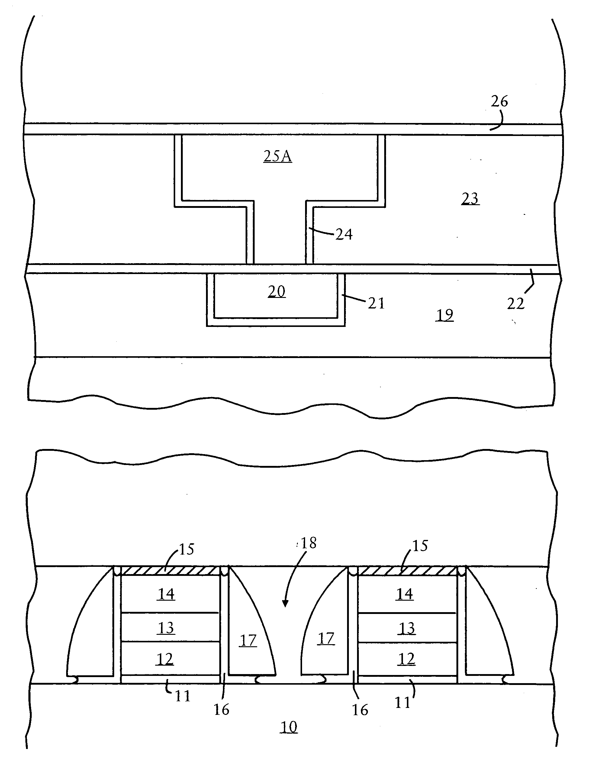
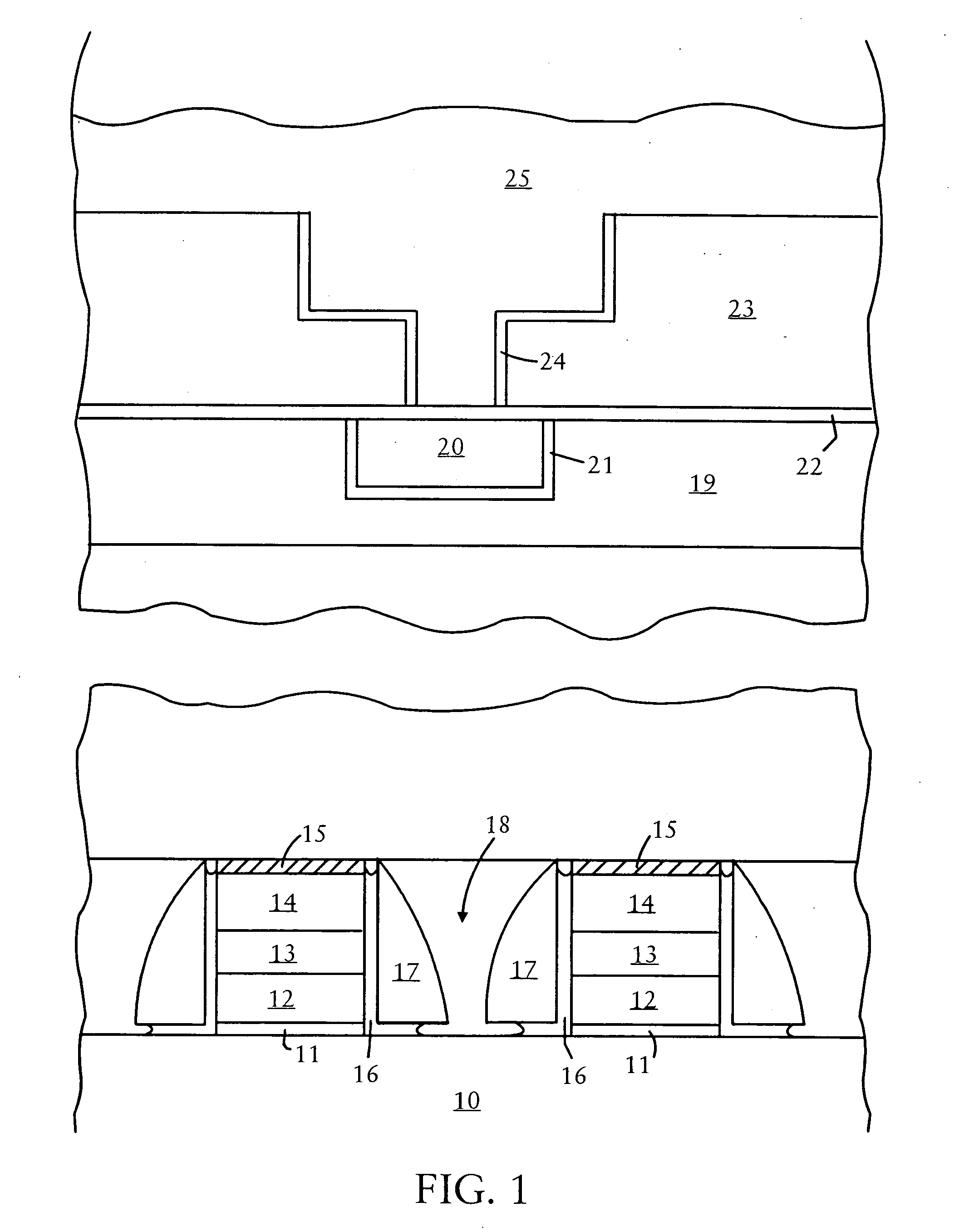
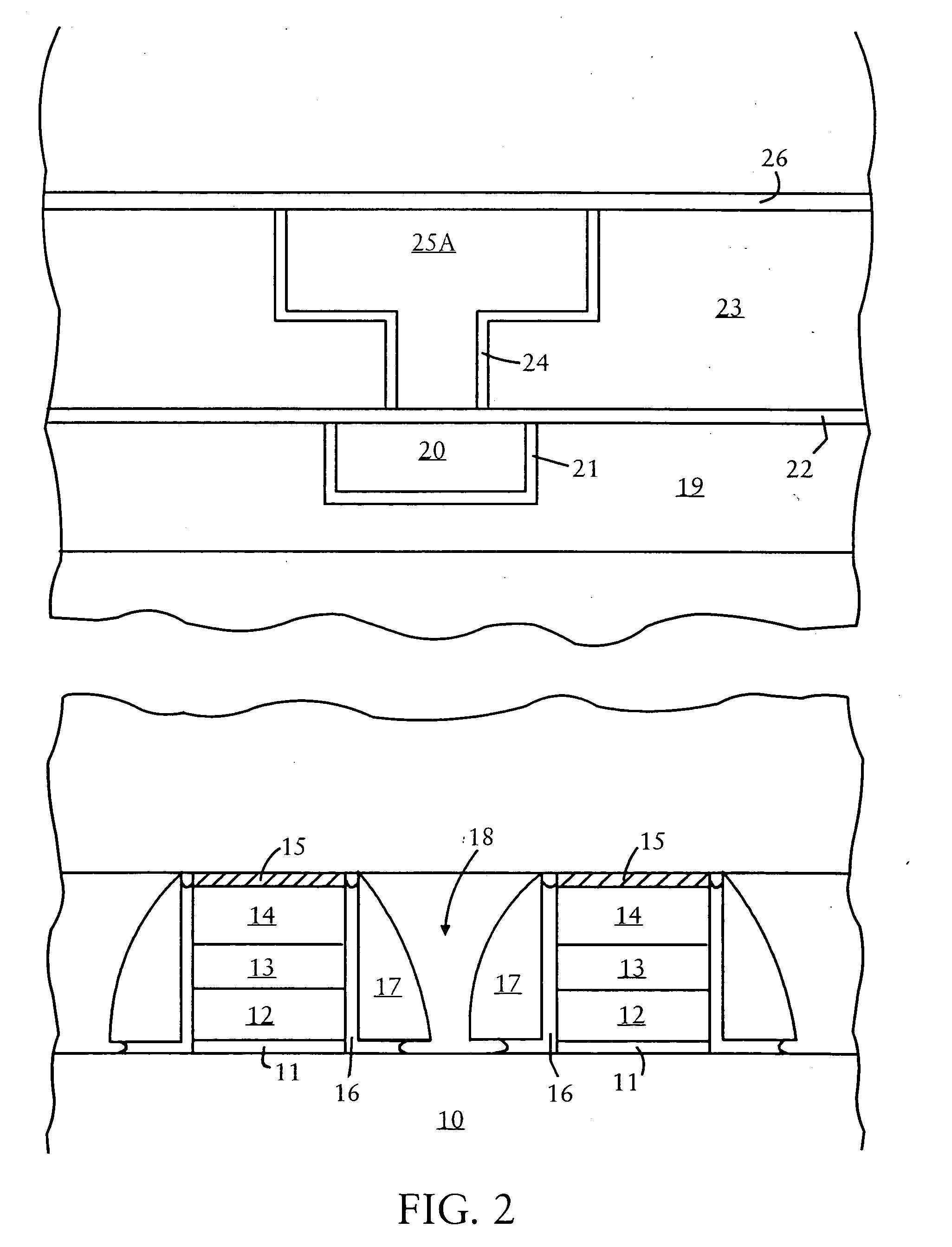
[0019]The present invention addresses and solves various reliability problems attendant upon conventional techniques for fabricating flash memory devices. These problems arise as semiconductor memory device dimensions continue to shrink, making it increasingly more difficult to effectively getter, reduce the generation of, and prevent the diffusion of mobile ion contaminants, such as hydrogen ions. The hydrogen ion contamination problem becomes exacerbated when integrating back end Cu interconnect technology with flash memory devices. During conventional back end processing, inlaid Cu is typically annealed in a forming gas atmosphere containing N2 and about 4 vol. % H2 at a temperature of about 250°. However, it was found that this process not only generated hydrogen ions but also accelerated the diffusion of hydrogen ions into the underlying devices, resulting in charge loss, adversely impacting data retention.

[0020]The present invention addresses and solves such data retention pro...


PUM

PropertyMeasurementUnit
temperatureaaaaaaaaaa

Abstract

Data retention in flash memory devices, such as mirrorbit devices, is improved by reducing the generation and / or diffusion of hydrogen ions during back end processing, such as annealing inlaid Cu. Embodiments include annealing inlaid Cu in an N2 atmosphere containing low H2 or no H2, and at temperatures less than 200° C., e.g., 100° C. to 150° C.

Description

FIELD OF THE INVENTION[0001]The present invention relates to a method of manufacturing semiconductor memory devices exhibiting high reliability and improved data retention. The present invention is particularly applicable to manufacturing high-speed integrated circuits in flash memory devices, with reduced charge loss.BACKGROUND OF THE INVENTION[0002]Semiconductor memory devices, such as erasable, programmable, read-only memories (EPROMs), electrically erasable programmable read-only memories (EEPROMs), and flash erasable programmable read-only memories (FEPROMs) are erasable and reusable, and are employed in various commercial electronic devices, such as computers, cellular telephones and digital cameras. There has recently evolved flash memory devices termed mirrorbit devices, which do not contain a floating gate electrode. In mirrorbit devices, the gate electrode is spaced apart from the substrate by an oxide / nitride / oxide (ONO) stack, such as a silicon oxide / silicon nitride / sili...

Claims


Application Information

Patent Timeline
Patent Type & Authority Applications(United States)
IPC IPC(8): H01L21/336H01L21/44
CPCH01L27/11521H01L21/76883H10B41/30
Inventor YOU, LUNICKEL, ALEXANDERTRAN, MINH Q.NGO, MINH-VANPHAM, HIEUWILSON, ERIKTOKUNO, HIROKAZUJAFARPOUR, AMIR HOSSEINKANG, INKUKHUERTAS, ROBERT
Owner ADVANCED MICRO DEVICES INC
Why Eureka
Try Eureka