Nanocomposite devices, methods of making them, and uses thereof

Inactive Publication Date: 2008-06-05
THE RES FOUND OF STATE UNIV OF NEW YORK
View PDF4 Cites 22 Cited by
  • Summary
  • Abstract
  • Description
  • Claims
  • Application Information

AI Technical Summary

Benefits of technology

[0013]As claimed in the present invention, nanocomposites formed by the addition of high-mobility semiconducting molecules and semiconducting nanoparticles to a polymer matrix exhibit enhanced photoconductive performance. In particular, efficient photogeneration of carriers coupled with enhanced conductance results in high photoconductive quantum efficiency in the present invention. The present invention combines broad spectral access and band gap tunability enabled by semiconducting nanoparticles (different compositions and sizes having different band gaps) with enhanced carrier transport via high-mobility semiconducting molecules in a polymeric matrix, to realize hybrid nanocomposites and devices. Moreover, the devices of the present invention can be prepared by solution phase incorporation and processing of organic and inorganic components. Thus, inexpensive, low temperatur

Problems solved by technology

The presently used conventional photodetector devices based on GaAs and AlGaAs depend on

Method used


Image

  • Nanocomposite devices, methods of making them, and uses thereof
  • Nanocomposite devices, methods of making them, and uses thereof
  • Nanocomposite devices, methods of making them, and uses thereof

Examples


example 1

Synthesis of PbSe Quantum Dots

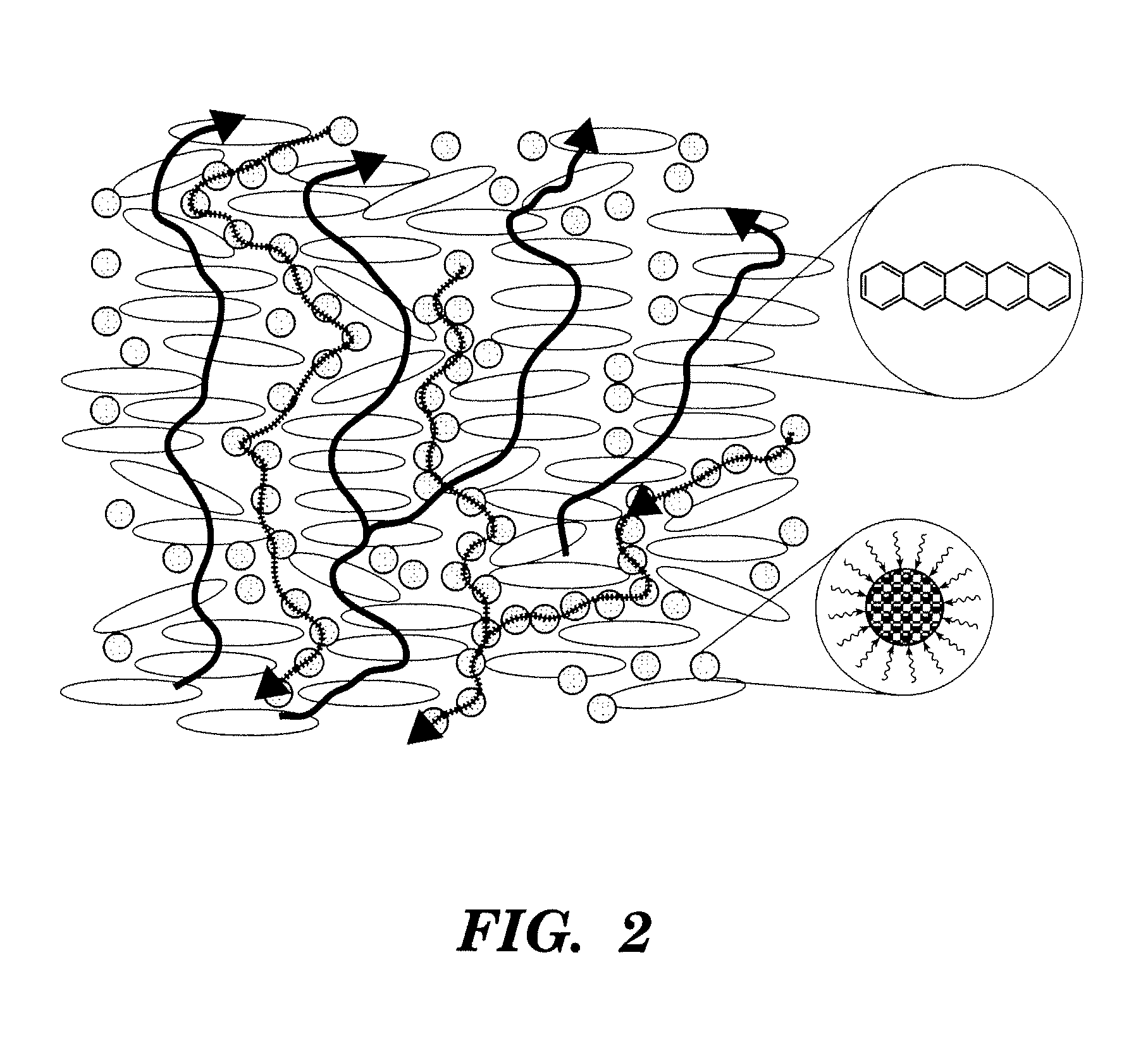
[0042]Discretely sized (Inset (b) of FIG. 3) PbSe QDs were prepared by a hot colloidal route using organically soluble precursors (Choudhury et al., “Efficient Photoconductive Devices at Infrared Wavelengths Using Quantum Dot-Polymer Nanocomposites,”Appl. Phys. Lett., 87:073110 (2005), which is hereby incorporated by reference in its entirety). PbO (5 mmol) and oleic acid (25 mmol) were added to 20 mL tri-n-octyylamine. The reaction mixture was heated under alternate vacuum and argon atmosphere for 30 minutes at 155° C., when 10 mL 1M TOP-Se (i.e. selenium dissolved in tri-n-octylphosphine) was rapidly injected into the reaction flask. The reaction took place instantaneously giving rise to uniform sized PbSe QDs. The product was syringed out in different fractions as a function of time from the reaction mixture and quenched in toluene. The QDs were cleaned off to remove excess surfactant oleic acid and other side products by precipitation with excess ac...

example 2

Preparation of a Soluble Precursor to Pentacene

[0043]The soluble pentacene precursor was prepared by the Diels-Alder reaction between pentacene and N-sulfinylacetamide, following Afzali et al., “High-Performance, Solution-Processed Organic Thin Film Transistors from a Novel Pentacene Precursor,”J. Am. Chem. Soc., 124(30): 8812-8813 (2002), which is hereby incorporated by reference in its entirety. In particular, N-sulfinylacetamide (840 mg, 8 mmol) was added to pentacene (556 mg, 2 mmol) and methyltrioxorhenium (30 mg, 0.12 mmol) in chloroform (30 mL). The mixture was refluxed for 12 hours and filtered after cooling. The product was purified by flash column chromatography (silica gel; chloroform). The resulting material was easily converted to pentacene by the retro Diels-Alder reaction under various backing temperatures, as shown in FIG. 4.

example 3

Introduction of Soluble Pentacene Precursor and Composite Device Fabrication

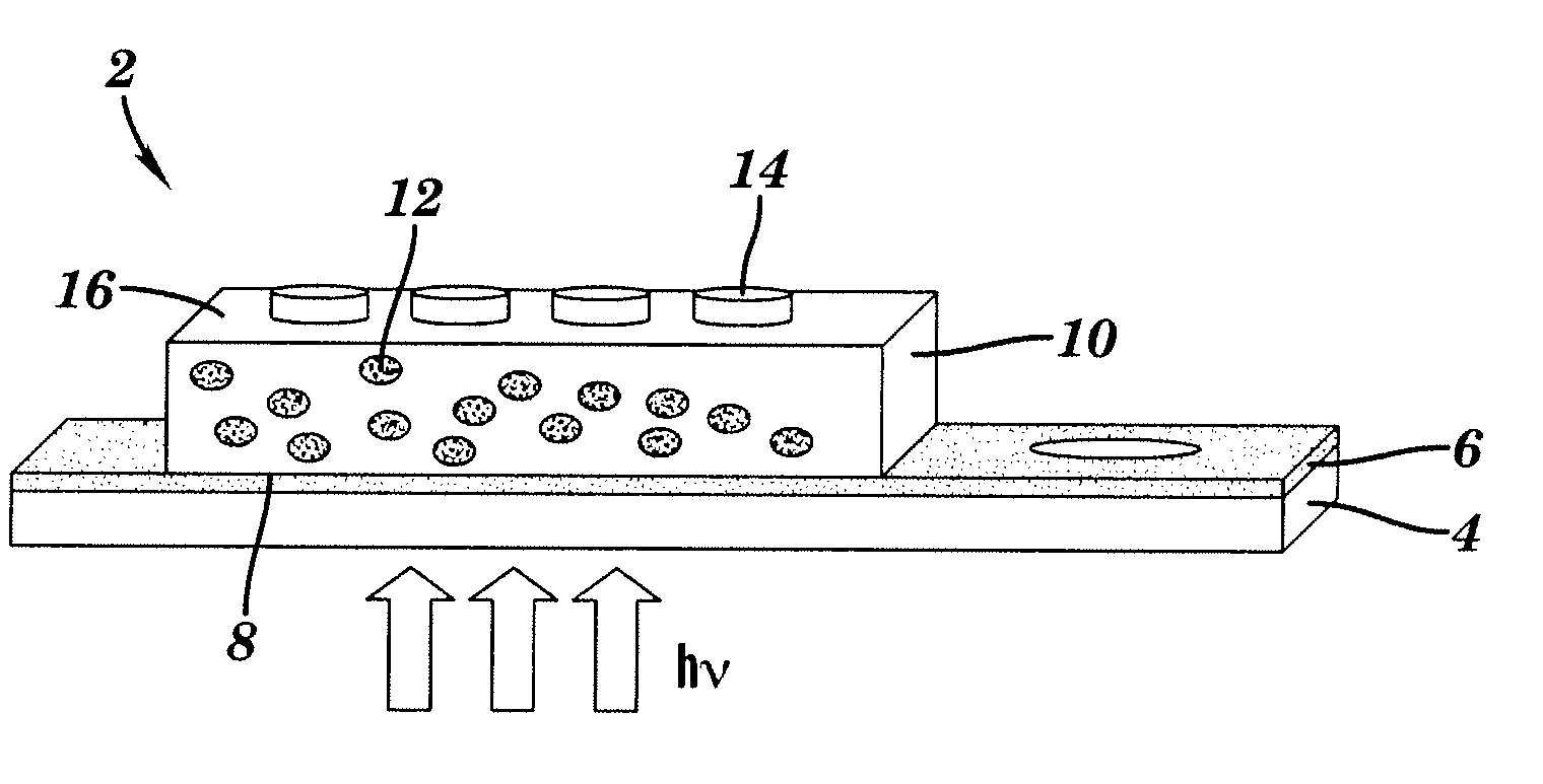
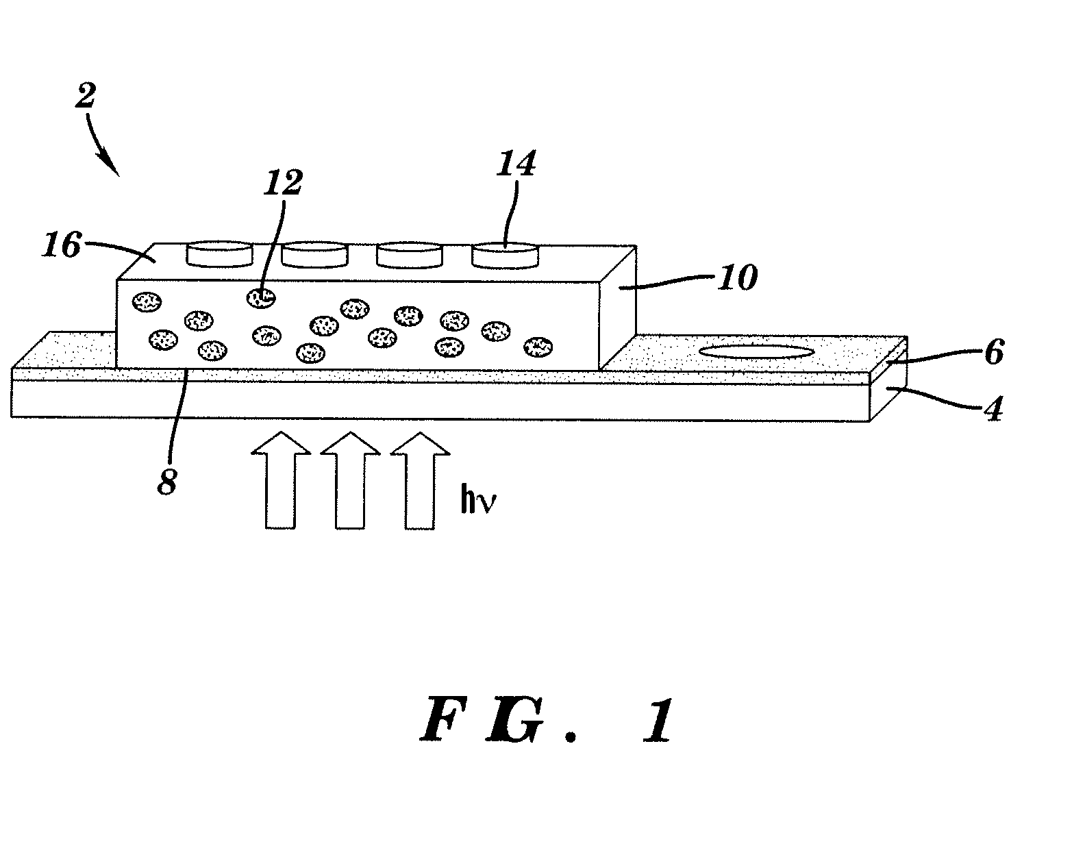
[0044]In a typical device fabrication procedure, the organic polymer PVK and the pentacene precursor in different proportions were dissolved in a known volume chloroform. Chloroform dispersions of oleic acid-capped PbSe QDs (with absorption tuned to 1340 nm) were then added and the composite solution was homogenized by vigorous stirring and ultrasonication, before being spin-cast on an indium tin oxide (ITO)-coated glass substrate to yield composite thin films. The resulting samples were dried overnight in vacuum to ensure complete solvent removal. Next, the dried films were annealed at 200° C. to let the precursor undergo thermolysis to generate pentacene in situ (FIG. 4). Finally, aluminum electrodes were thermally evaporated through a shadow mask to yield devices with active area ˜0.04 cm2 (FIG. 1). The average thickness of the composite film was determined to be about 100 nm.

[0045]The absorption spectra ...


PUM

PropertyMeasurementUnit
Areaaaaaaaaaaa
Polymericaaaaaaaaaa
Semiconductor propertiesaaaaaaaaaa

Abstract

The present invention relates to a nanocomposite device comprising a polymeric matrix, semiconducting nanoparticles, and a semiconducting molecule having a field-effect mobility of at least 0.1 cm2/Vs. In addition, the present invention relates to a method of making a nanocomposite device. The method includes providing a mixture comprising a polymer, semiconducting nanoparticles, and a semiconducting molecule having a field-effect mobility of at least 0.1 cm2/Vs or a soluble precursor thereof, depositing the mixture on a substrate, and treating the mixture under conditions effective to produce a nanocomposite device comprising the polymeric matrix, semiconducting nanoparticles, and the semiconducting molecule having a field-effect mobility of at least 0.1 cm2/Vs. Thin film devices including the nanocomposite device are also disclosed.

Description

[0001]This application claims the benefit of U.S. Provisional Patent Application Ser. No. 60 / 824,686, filed Sep. 6, 2006, which is hereby incorporated by reference in its entirety.[0002]The subject matter of this application was made with support from the United States Government under the National Science Foundation, Grant No. DMR0318211 and AFOSR Grant No. F496200110358. The U.S. Government may have certain rights.FIELD OF THE INVENTION[0003]The present invention relates to a nanocomposite device comprising a polymeric matrix, semiconducting nanoparticles, and a semiconducting molecule having a field-effect mobility of at least 0.1 cm2 / Vs. In addition, the present invention relates to a method of making a nanocomposite device. The method includes providing a mixture comprising a polymer, semiconducting nanoparticles, and a semiconducting molecule having a field-effect mobility of at least 0.1 cm2 / Vs or a soluble precursor thereof, depositing the mixture on a substrate, and treatin...

Claims


Application Information

Patent Timeline
IPC IPC(8): H01L31/04B05D5/12
CPCB82Y30/00H01L51/0035H01L51/0036Y02E10/549H01L51/0042H01L51/426H01L51/0038Y02P70/50H10K85/111H10K85/114H10K85/146H10K85/113H10K30/35
Inventor CHOUDHURY, KAUSHIK ROYKIM, WON JINSAHOO, YUDHISTHIRALEE, KWANG SUPPRASAD, PARAS N.CARTWRIGHT, ALEXANDERTHAPA, RAM B.
Owner THE RES FOUND OF STATE UNIV OF NEW YORK
Why Eureka
Try Eureka