Apparatus and Method for Measuring Curvature Using Multiple Beams

a technology of curvature and beam, applied in the direction of force measurement by measuring optical property variation, instruments, lasers, etc., can solve the problems of failure of interconnection or thin film strip, deterioration of device performance, and inability to achieve desired stress changes in any stage of thin film fabrication process, so as to reduce the size of curvature measuring apparatus, and simplify the structure

Inactive Publication Date: 2008-08-07
NANOTRON GES FUR MIKROTECHN
View PDF6 Cites 37 Cited by
  • Summary
  • Abstract
  • Description
  • Claims
  • Application Information

AI Technical Summary

Benefits of technology

[0026]The curvature measuring apparatus according to the present invention has a simpler structure than the conventional apparatus. In order to apply the apparatus for measuring the curvature or the stress in real time to thin film deposition equipments, the reduction in size of the curvature measuring apparatus is a critical technical issue. In the present invention, it is possible to reduce the size of the curvature measuring apparatus to a palm size by using the VCSEL array or the LD array by removing complicated mechanical structures and optical parts used in the multiple beam method using etalons or in the laser scanning system.
[0027]According to the present invention, since an m×n light source array (an m×n VCSEL array or an m×n LD array) is used to obtain multiple beams, the intensity of the laser beam is not reduced unlike the conventional curvature measuring method using the high-reflectivity etalon. When the conventional high-reflectivity etalon is used, the laser beam of which the intensity is reduced to 1/10000 or less strikes the substrate. Even if the intensity of the laser beam of the m×n light source array used in

Problems solved by technology

The undesirable change in stress may occur in any stage of the thin film fabrication process.
The stress can cause the deterioration of a device performance, the failure of an interconnection or the strip of the thin film.
Since the method using the X-ray uses a lattice diffraction phenomenon, the method is hard to apply to every thin film.
In addition, there is a difficulty in quantification when the stress is measured in real time.
However, since this method measures the curvature while moving the laser beam on the wafer, this method is apt to be influenced by external vibration or noise during the measurem

Method used


Image

  • Apparatus and Method for Measuring Curvature Using Multiple Beams
  • Apparatus and Method for Measuring Curvature Using Multiple Beams
  • Apparatus and Method for Measuring Curvature Using Multiple Beams

Examples


first embodiment

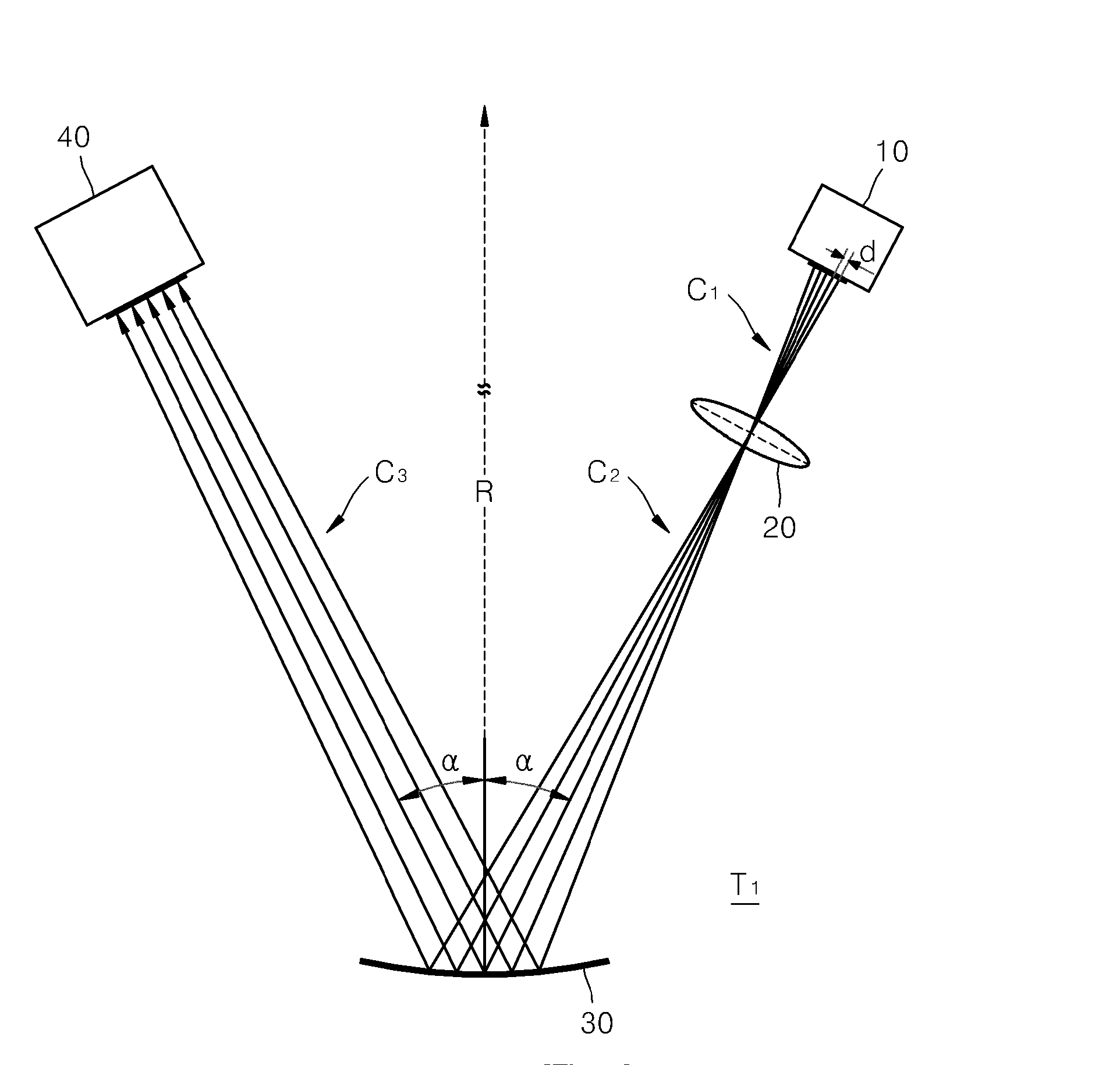
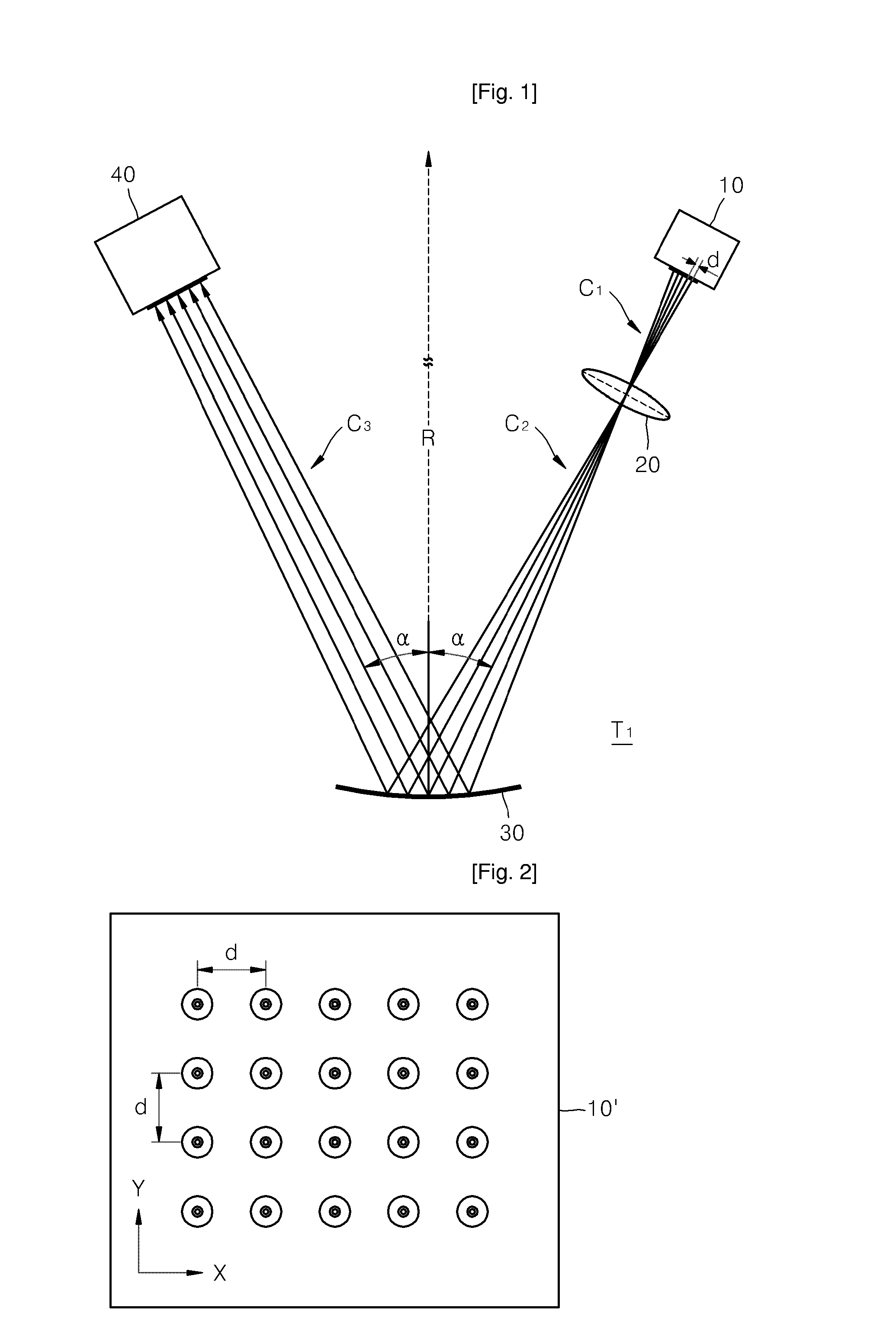
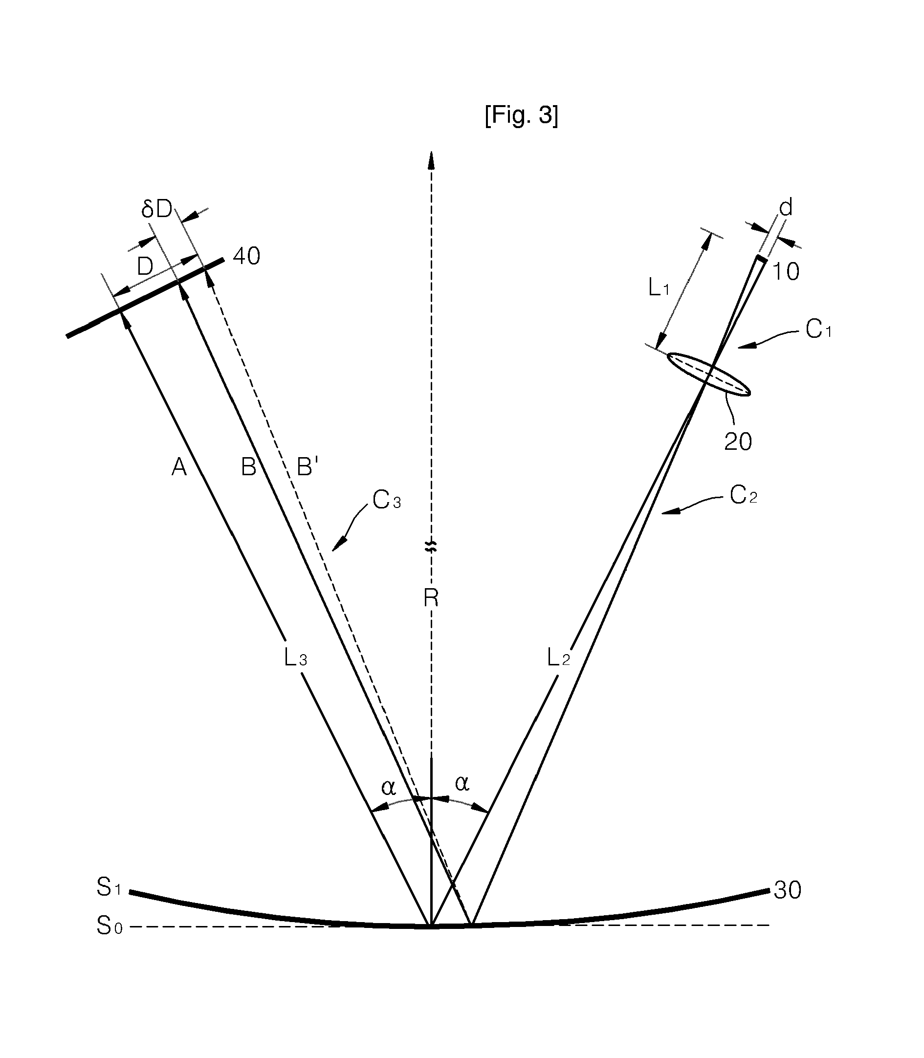
[0040]FIG. 1 is a schematic view of a curvature measuring apparatus T1 using m×n multiple divergent beams according to a first embodiment of the present invention (here, m and n are from 1 to 100, respectively).

[0041]A reference numeral 10 of FIG. 1 is an m×n light source array which is any one of an m×n laser diode (LD) array and an m×n vertical cavity surface emitting laser (VCSEL) array having a pitch d. The m×n light source array 10 generates m×n laser beams C1. FIG. 2 shows a 5×4 VCSEL array 10′ having a uniform pitch d. X direction correspond to the direction parallel to the incident plane of laser beams and Y direction correspond to the direction perpendicular to the incident plane of lasers beams.

[0042]The m×n laser beams C1 generated by the m×n light source array 10 is collimated by a single collimating lens unit 20 to form m×n multiple divergent beams C2. The single collimating lens unit 20 includes at least one aspherical optical lens for reducing aberration. The single c...

second embodiment

[0051]FIG. 4 is a schematic view of a curvature measuring apparatus T2 which strikes m×n multiple divergent beams at normal incidence according to a second embodiment of the present invention.

[0052]First, an m×n light source array 110 which is any one of an m×n LD array and an m×n VCSEL array having a pitch d generates m×n laser beams D1.

[0053]A single collimating lens unit 120 receives the m×n laser beams D1 and generates m×n multiple divergent beams D2 having a uniform divergence angle. The single collimating lens unit 120 includes at least one aspherical optical lens for reducing aberration. The single collimating lens unit 120 may further include a focusing lens.

[0054]Next, the m×n multiple divergent beams D2 are incident on the surface of a substrate 130 through a beam splitter 160 at normal incidence.

[0055]The beam splitter 160 splits m×n multiple beams D3 reflected from the surface of the substrate 130 at a right angle from the incident beams D2. The split m×n multiple beams ...

third embodiment

[0060]FIG. 5 is a schematic view of a curvature measuring apparatus T3 for forming m×n multiple parallel beams using an m×n microlens array and measuring curvature according to a third embodiment of the present invention.

[0061]A reference numeral 210 of FIG. 5 is an m×n light source array which is any one of an m×n LD array and an m×n VCSEL array having a pitch d. The LD array outputs elliptical beams. Accordingly, when the m×n LD array is used, the elliptical beams must be converted into circular beams using a micro lens array.

[0062]The m×n light source array 210 generates m×n laser beams E1 and the m×n laser beams E1 are converted into m×n multiple parallel beams E2by an m×n micro collimating lens array unit 270. The laser beams generated by the m×n light source array 210 is converted into parallel laser beams using a micro collimating lens array.

[0063]The m×n multiple parallel beams E2 are incident on surface of a substrate 230 at an incident angle a (from equal to or more than 0...


PUM


Abstract

There is provided a curvature measuring apparatus and method using multiple beams. m×n multiple beams generated by an m×n laser diode (LD) array or an m×n vertical cavity surface emitting laser array having a uniform pitch are converted into multiple divergent or multiple parallel beams. The multiple beams strike and reflect from the surface of a thin film formed on a substrate Then, the multiple beams are detected by an m×n spot array in a detector such as a charge coupled device (CCD) or a CMOS image sensor. The spot spacing between the beams in the array is measured in a direction parallel to the incident plane. The spot spacing between the beams is changed by the curvature of the substrate in the direction parallel to the incident plane and the curvature may be expressed by a function including change in beam spacing, an incident angle, a distance between the surface of the thin film and the detector. These values can be measured and the curvature of the surface of the thin film can be obtained from these values. Since an m×n two-dimensional spot array is used, it is possible to obtain a two-dimensional curvature profile of the surface of the thin film.

Description

TECHNICAL FIELD[0001]The present invention relates to a technology of measuring the curvature of a substrate and the stress of a thin film formed on the substrate, and more particularly, to an apparatus and method for measuring the curvature of a substrate using multiple beams for the purpose of calculating the stress of a thin film.BACKGROUND ART[0002]When a thin film such as a semiconductor epitaxial layer is grown, large stress occurs in the thin film, which changes the property of the thin film. The undesirable change in stress may occur in any stage of the thin film fabrication process. The stress can cause the deterioration of a device performance, the failure of an interconnection or the strip of the thin film. Accordingly, in order to achieve desired optical, electric and mechanical properties of the thin film, the thin film stress must be measured and controlled.[0003]In general, the stress of the thin film is intimately associated with a thin film growth mechanism, a grown...

Claims


Application Information

Patent Timeline
IPC IPC(8): G01B11/14G01B11/24
CPCG01B11/25G01L1/24H01S5/4025
Inventor KEE, BONGYOON, EUI-JOON
Owner NANOTRON GES FUR MIKROTECHN
Why Eureka
Try Eureka