Wavelength Converter, Light-Emitting Device, Method of Producing Wavelength Converter and Method of Producing Light-Emitting Device

a technology of light-emitting devices and wavelength converters, which is applied in the manufacture of electric discharge tubes/lamps, discharge tubes luminescent screens, instruments, etc., to achieve the effects of inhibiting the deterioration of fluorescence characteristics, reducing self-quenching of phosphors, and high luminous efficiency

Inactive Publication Date: 2008-09-25
KYOCERA CORP
View PDF9 Cites 186 Cited by
  • Summary
  • Abstract
  • Description
  • Claims
  • Application Information

AI Technical Summary

Benefits of technology

[0026]The main advantage of the present invention is to provide a wavelength converter useful for a light-emitting device which reduces self-quenching of phosphors and has high luminous efficiency, and a light-emitting device using the same.
[0027]Another advantage of the present invention is to provide a wavelength converter wherein the use of semiconductor ultrafine particles having a mean particle size of not more than 20 nm inhibits fluorescence characteristics from deteriorating due to moisture and the semiconductor ultrafine particles are dispersed as individual particles in resin without aggregating, and a light-emitting device using the same.
[0028]The other advantage of the present invention is to provide a wavelength converter that has high performance and stability over a long period of time without lowering...

Problems solved by technology

However, the problem is that if brilliance of the LED light-emitting element 23 is changed, the light quantity ratio of blue to yellow changes and therefore white color tone changes, leading to poor color rendering.
Although the light-emitting device described in Patent literature 2 covers a wide range of emission wavelengths and therefore significantly improves color rendering, there has been the problem that luminous efficiency is lowered as a whole because the presence of three types of phosphors 25 mixed in the wavelength conversion layer 23 causes interaction between phosphors such as a red phosphor absorbing the light converted by a blue phosphor, inducing self-quenching, and the light once converted is absorbed by phosphors again.
Consequently, emission intensity is not sufficient and the light-emitting device is made dark.
Furthermore, such a system as described in Patent literature 3 has had the problem that the luminous efficiency (fluorescence quantum yield) of phosphors is low and in particular, the luminous efficiency of red in the range of 600 to 750 nm is low.
However, as mentioned below, there are two problems with semiconductor particles having smaller particle size.
The first problem is that semiconductor particles having a particle size as small as about 20 nm ends up having a high ratio of the surface area to the volume and therefore the particle surface reacts with water, deteriorating fluorescence characteristics.
However, there is the problem that phosphors react with moisture in the process before mixing phosphors with resin and hardening them, det...

Method used


Image

  • Wavelength Converter, Light-Emitting Device, Method of Producing Wavelength Converter and Method of Producing Light-Emitting Device
  • Wavelength Converter, Light-Emitting Device, Method of Producing Wavelength Converter and Method of Producing Light-Emitting Device
  • Wavelength Converter, Light-Emitting Device, Method of Producing Wavelength Converter and Method of Producing Light-Emitting Device

Examples


example 1

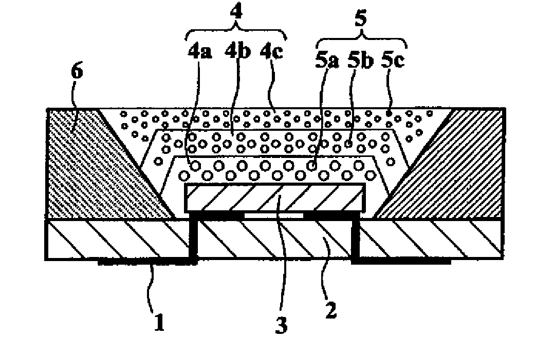
[0179]A light-emitting device in FIG. 1 was produced. First, a light-emitting element composed of nitride semiconductor was formed on a light-emitting element substrate composed of sapphire through metal organic chemical vapor deposition method.

[0180]As the structure of the light-emitting element, n-type GaN layer which is undoped nitride semiconductor, GaN layer as n-type contact layer having an n-type electrode of Si dope, n-type GaN layer which is undoped nitride semiconductor, GaN layer as barrier layer constituting an emission layer, InGaN layer constituting a well layer and GaN layer as barrier layer were formed as one set on a light-emitting element substrate, and multiquantum well structure wherein the InGaN layer sandwiched by GaN layers was composed of five stacked layers was adopted.

[0181]The light-emitting element was mounted in a package wherein an insulating substrate having wiring pattern for disposing a near-ultraviolet LED formed, and a flame-like reflection member ...

example 2

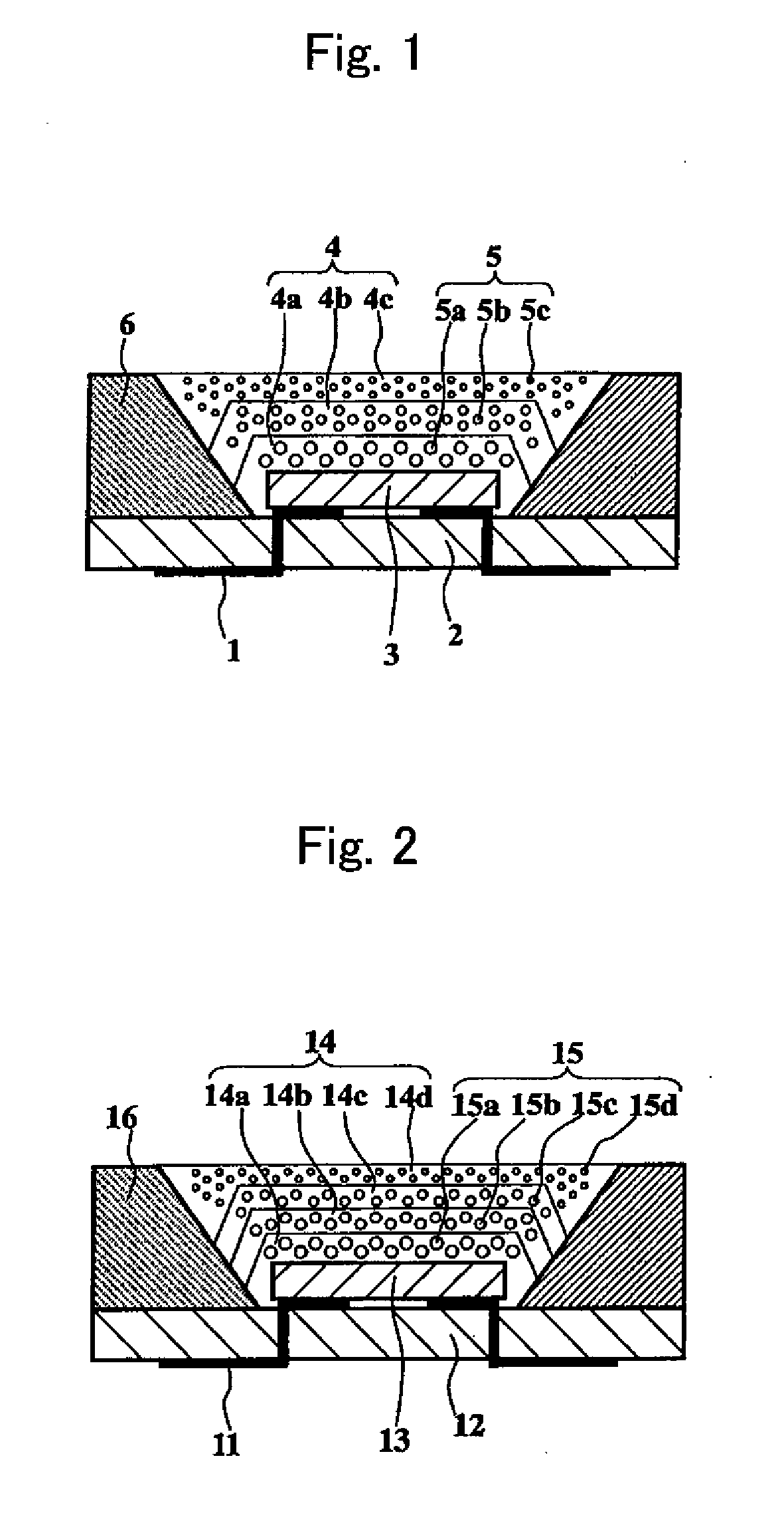
[0197]A light-emitting device was produced through the following method. First, a light-emitting element composed of nitride semiconductor was formed on a light-emitting element substrate composed of sapphire through metal organic chemical vapor deposition method.

[0198]As the structure of the light-emitting element, n-type GaN layer which is undoped nitride semiconductor, GaN layer as n-type contact layer having an n-type electrode of Si dope, n-type GaN layer which is undoped nitride semiconductor, GaN layer as barrier layer constituting an emission layer, InGaN layer constituting a well layer and GaN layer as barrier layer were formed as one set on a light-emitting element substrate, and multiquantum well structure wherein the InGaN layer sandwiched by GaN layers was composed of five stacked layers was adopted.

[0199]The light-emitting element was mounted in a package wherein an insulating substrate having wiring pattern for disposing a near-ultraviolet LED formed, and a flame-like...

example 3

[0206]With regard to semiconductor ultrafine particles CdSe used in Example 2, changing the type of surface-modifying molecules, luminescence characteristics of semiconductor ultrafine particles were evaluated.

[0207]First, a method of producing CdSe ultrafine particles that are semiconductor ultrafine particles will be described. 7.9 g (0.1M) of Se powder manufactured by Kanto Chemical Co., Inc. was dissolved in 250 g of trioctylphosphine (TOP), and this was named Solution 1. Next, 7.6 g (0.1M) of sodium sulfide manufactured by Kanto Chemical Co., Inc. was dissolved in 250 g of trioctylphosphine (TOP), and this was named Solution 2.

[0208]Then, 5.3 g (0.02M) of cadmium acetate manufactured by Kanto Chemical Co., Inc. and 100 g of stearic acid were mixed and dissolved at 130° C. 400 g of trioctylphosphineoxide (TOPO) was added to this solution, heated to 300° C. and dissolved.

[0209]The above Solution 1 was added to this solution and reacted under the condition of 300° C. After complet...


PUM


Abstract

A light-emitting device comprises a light-emitting element 3 that is provided on a substrate 2 and emits excitation light, and a wavelength converter 4 that converts the excitation light into visible light. The visible light is output light. The wavelength converter 4 comprises a plurality of wavelength conversion layers 4a, 4b and 4c which respectively contain, as phosphors, at least one type of semiconductor ultrafine particles having a mean particle size of not more than 20 nm and at least one type of fluorescent substance having a mean particle size of not less than 0.1 μm in a resin matrix. Thereby, self-quenching of phosphors is reduced and high luminous efficiency is attained.

Description

TECHNICAL FIELD[0001]The present invention relates to a wavelength converter used for a light-emitting device and the like to wavelength-convert light emitted from a light-emitting element and take it to the outside, a light-emitting device, a method of producing a wavelength converter and a method of producing a light-emitting device. In particular, it relates to a wavelength converter suitably used for backlight power supply for electronic display, fluorescent lamps or the like, a light-emitting device, a method of producing a wavelength converter and a method of producing a light-emitting device.BACKGROUND ART[0002]A light-emitting element (hereinafter, referred to also as LED chip) made of semiconductor material has small size and good power efficiency, and becomes brilliantly colored. In addition, because of its excellent characteristics such as long product life, resistance to on / off lighting repetition and low power consumption, an LED chip is expected to be applied to a back...

Claims


Application Information

Patent Timeline
IPC IPC(8): H01J1/62G03C5/00H01J9/02C09K11/08C09K11/56C09K11/58C09K11/59C09K11/64C09K11/70C09K11/77C09K11/88H01L33/50
CPCC09K11/565H01L33/504C09K11/595C09K11/642C09K11/643C09K11/703C09K11/7734C09K11/7739C09K11/7771C09K11/7774C09K11/7777C09K11/7787C09K11/7789C09K11/7794C09K11/7797C09K11/883H01L33/502C09K11/584H01L2224/16225H01L2924/00014H01L2924/00011H01L2224/0401
Inventor MASATO, FUKUDOMETOSHIAKI, SHIGEOKAFUJITO, NAKAGAWAJITETSUAKI, OZAKI
Owner KYOCERA CORP
Why Eureka
Try Eureka