Phosphorescent OLED with mixed electron transport materials

a technology of electron transport materials and phosphorescent oled, which is applied in the direction of discharge tube luminescnet screens, other domestic articles, natural mineral layered products, etc., can solve the problems of large loss of efficiency, large excitons, and performance limitations of oled devices, and achieve the effect of reducing the drive voltage of oled devices

Active Publication Date: 2008-10-23
GLOBAL OLED TECH
View PDF13 Cites 20 Cited by
  • Summary
  • Abstract
  • Description
  • Claims
  • Application Information

AI Technical Summary

Benefits of technology

[0029]Devices of the invention provide reduced drive voltage of OLED devices, and provide embodiments with other improved features such as operational stability and luminance

Problems solved by technology

While organic electroluminescent (EL) devices have been known for over two decades, their performance limitations have represented a barrier to many desirable applications.
However, only 25% of the excitons created in an EL device are singlet excitons.
This results in a large loss in efficiency since 75% of the excitons are not used in the light emission process.
rity. However, in this case, blue OLED devices employing these disclosed materials require use of substantial amounts of the phosphorescent emitters and still do not solve the high voltage pr
The document describes that devices utilizing plural host compounds show higher current and higher efficiencies at a given voltage; however, reported luminance data are quite moderate.
However, use of these materials alone does not give the optimum performance possible in an electroluminescent device.
However, the Bphen / Alq mix of Seo et al., shows inferior stability.
However, these devices do not have all desired EL characteristics in terms of high luminance and stability of the components in combination with low drive voltages.

Method used


Image

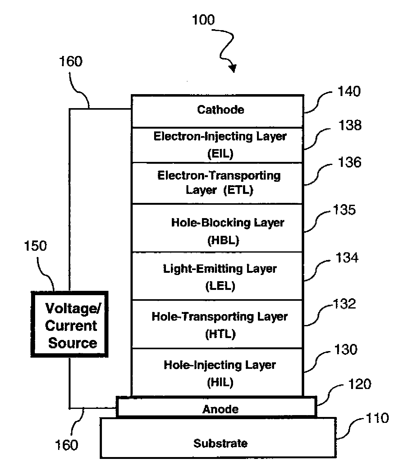
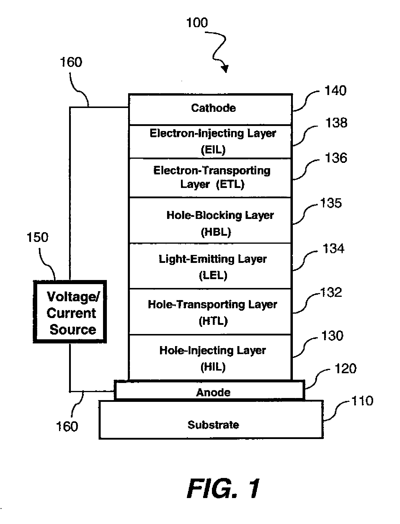
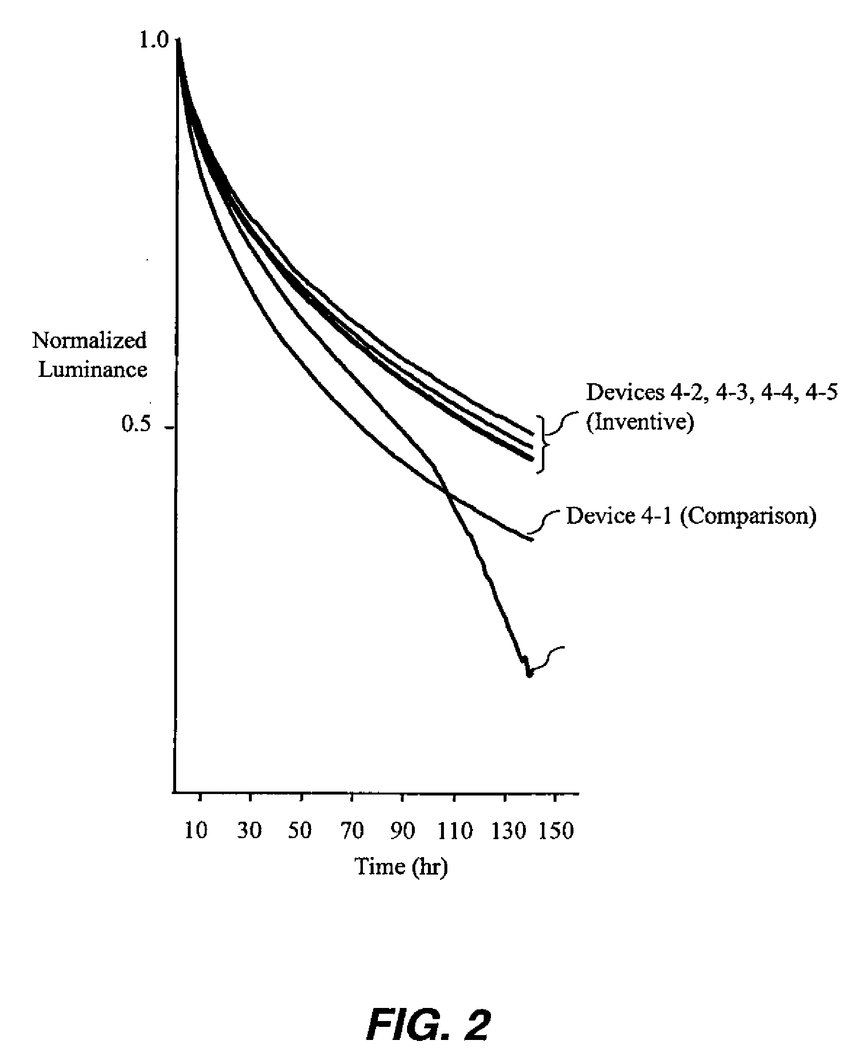
  • Phosphorescent OLED with mixed electron transport materials
  • Phosphorescent OLED with mixed electron transport materials
  • Phosphorescent OLED with mixed electron transport materials

Examples


example 1

Synthesis of Compound A-16

[0314]

[0315]Compound (3), eq. 1, was prepared in the following manner. Under a nitrogen atmosphere, acetylenic compound (2) (2.0 g, 12 mMole), was dissolved in dimethylformamide (DMF) (100 mL) and the solution cool to 0° C. Potassium t-butoxide (KButO) (1.4 g, 12 mMole), was added and the mixture stirred well for approximately 15 minutes. To this mixture was then added the benzophenone (1) (3.53 g, 30 mMole). Stirring was continued at 0° C. for approximately 30 minutes and then allowed to come to room temperature over a 1-hour period. At the end of this time the solution was cooled to 0° C. and the reaction treated with saturated sodium chloride (20 mL). The mixture was then diluted with ethyl acetate, washed with 2N—HCl (3 times), dried over MgSO4, filtered and concentrated under reduced pressure. The crude product was triturated with petroleum ether to give the product as an off-white solid. The yield of compound (3) was 3.0 g.

[0316]Compound (3) (7.0 g, 1...

example 2

Determination of LUMO Values

[0317]An important relationship exists when selecting the first compound and second compound(s) of the invention. A comparison of the LUMO values of the first and second compounds in the layer of the invention must be carefully considered. To obtain a drive voltage reduction over devices that contain only a first compound or only a second compound, there must be a difference in the LUMO values of the compounds. The first compound must have a lower LUMO (more negative) value than the second compound, or compounds.

[0318]The LUMO values are typically determined experimentally by electrochemical methods. A Model CH1660 electrochemical analyzer (CH Instruments, Inc., Austin, Tex.) was employed to carry out the electrochemical measurements. Cyclic voltammetry (CV) and Osteryoung square-wave voltammetry (SWV) were used to characterize the redox properties of the compounds of interest. A glassy carbon (GC) disk electrode (A=0.071 cm2) was used as working electrod...

example 3

Determination of Low-Voltage Electron Transport Materials

[0320]Materials were tested to determine if they were low voltage electron transport materials by incorporating them alone into the electron-transporting layer of a device. Devices were constructed in the following manner.

[0321]A glass substrate coated with an 85 nm layer of indium-tin oxide (ITO) as the anode was sequentially ultrasonicated in a commercial detergent, rinsed in deionized water, degreased in toluene vapor and exposed to oxygen plasma for about 1 min.

[0322]a) Over the ITO was deposited a 1 nm fluorocarbon (CFx) hole-injecting layer (HIL) by plasma-assisted deposition of CHF3.

[0323]b) A hole-transporting layer (HTL) of N,N′-di-1-naphthalenyl-N,N′-diphenyl-4,4′-diaminobiphenyl (NPB) having a thickness of 75 nm was then evaporated onto a).

[0324]c) A 35 nm light-emitting layer (LEL) of tris(8-quinolinolato)aluminum (III) (Alq) was then deposited onto the hole-transporting layer.

[0325]d) A 35 nm electron-transporting...


PUM

PropertyMeasurementUnit
work functionaaaaaaaaaa
thickaaaaaaaaaa
operating voltagesaaaaaaaaaa

Abstract

An OLED device comprising, in sequence, an anode, a light-emitting layer that comprises a phosphorescent light-emitting organometallic compound, a hole-blocking layer, and a cathode, and between the hole-blocking layer and the cathode, a further layer containing a mixture of a first compound that is a tetracene compound that has the lowest LUMO value of the compounds in the layer, in an amount greater than or equal to 10% and less than 90% and a second compound that is a low voltage electron transport material, exhibiting a higher LUMO value than the first compound in an amount less than or equal to 90% and more than 10%.

Description

CROSS-REFERENCE TO RELATED APPLICATION[0001]This is a continuation of U.S. application Ser. No. 11 / 116,096, filed on Apr. 27, 2005, by William J. Begley, et al, the disclosure of which is incorporated by reference. Reference is made to commonly assigned U.S. Ser. Nos. 11 / 076,821 and 11 / 077,218 filed on Mar. 10, 2005, by William J. Begley, et al., entitled “Organic Light-Emitting Devices With Mixed Electron Transport Materials” the disclosure of which is incorporated herein by reference.FIELD OF THE INVENTION[0002]This invention relates to an organic light-emitting diode (OLED) electroluminescent (EL) device having a light-emitting layer including a phosphorescent light-emitting material and a layer between the light-emitting layer and the cathode containing a mixture of at least two compounds.BACKGROUND OF THE INVENTION[0003]While organic electroluminescent (EL) devices have been known for over two decades, their performance limitations have represented a barrier to many desirable a...

Claims


Application Information

Patent Timeline
Patent Type & Authority Applications(United States)
IPC IPC(8): H01L51/50
CPCC09K11/06C09K2211/1007C09K2211/1011C09K2211/1014C09K2211/1029C09K2211/1044C09K2211/1059C09K2211/107C09K2211/1088C09K2211/186C09K2211/188H01L51/0052H01L51/0053H01L51/0058H01L51/0081H01L51/0085H01L51/5016H01L51/5036H01L2251/308H05B33/14Y10S428/917H10K85/621H10K85/615H10K85/626H10K85/324H10K85/342H10K50/125H10K50/11H10K2101/10H10K2102/103
Inventor BEGLEY, WILLIAM J.HATWAR, TUKARAM K.DEATON, JOSEPH C.BROWN, CHRISTOPHER T.ANDRIEVSKY, NATASHAKONDAKOVA, MARINA E.
Owner GLOBAL OLED TECH
Why Eureka
Try Eureka