
Method and process for forming a self-aligned silicide contact

a metal silicide and contact technology, applied in the direction of semiconductor devices, basic electric elements, electrical equipment, etc., can solve the problems of increasing the difficulty of forming shallow junctions for silicon-on-insulator (soi) substrates, sub>2 /sub>also exhibits rapid sheet resistance degradation, and shortening the device between the gate and the source/drain region

Inactive Publication Date: 2008-11-06
TAIWAN SEMICON MFG CO LTD
View PDF7 Cites 27 Cited by
  • Summary
  • Abstract
  • Description
  • Claims
  • Application Information

AI Technical Summary

Benefits of technology

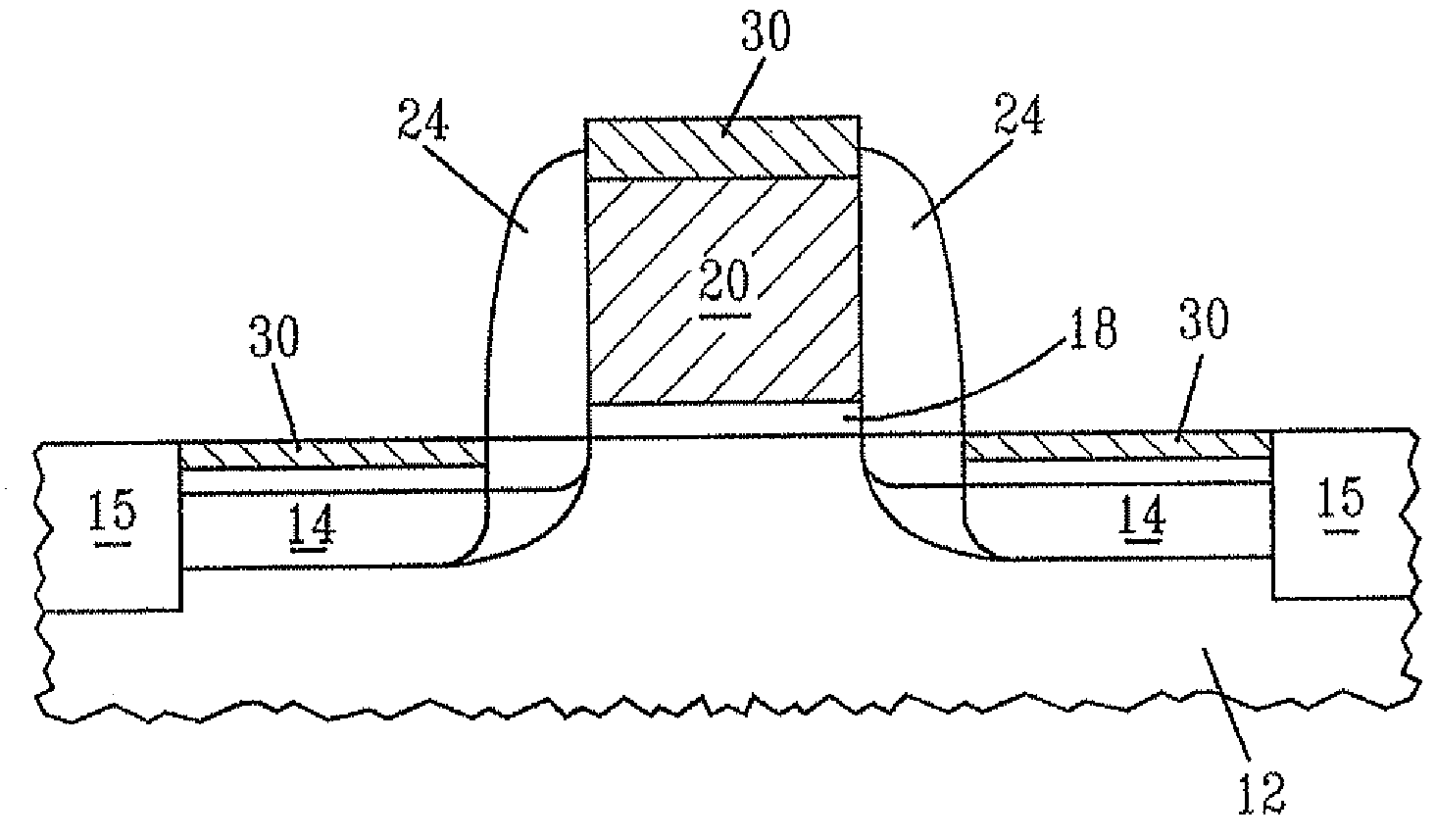
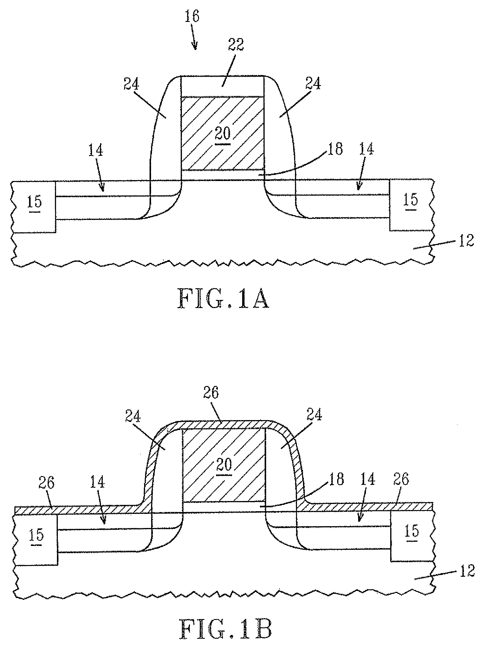
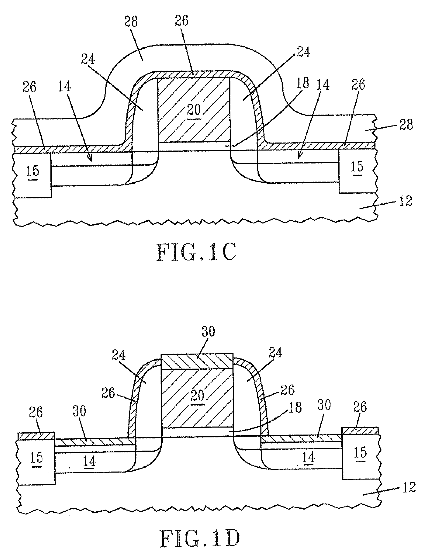
The present invention provides a method for forming a self-aligned NiSi, PtSi contact by depositing a blanket layer of Ni with Pt over a surface of a structure including at least one gate region, forming an oxygen diffusion barrier layer, and heating the structure to a temperature to form a NiSi, PtSi contact on portions of the structure comprising silicon. The method uses an etching process that selectively removes unreacted metals from the surface of the structure while not attacking the metal silicide contacts. The method also includes optimizing the annealing conditions to form optimal contacts. The invention also provides a method for etching a NiPt alloy selective to NiSi, PtSi.

Problems solved by technology

However, CoSi2 consumes significant amounts of silicon during formation, which increases the difficulty of forming shallow junctions for silicon-on-insulator (SOI) substrates.
Further, as the semiconductor industry approaches dimensions less than 65 nm, CoSi2 also exhibits rapid sheet resistance degradation.
Further, when shallow junctions (on the order of about 15 nm or less) are to be formed, nickel disilicide formation is seen under the spacer resulting in shorting of the device between the gate and the source / drain regions.
Such etchants are incapable of removing all additional elements especially noble metals such as Pt, Pd, Rh and Re used along with Ni.
Presence of the unreacted metal on the spacers and trench isolation regions leads to shorting of the devices thereby preventing the manufacturing of a functioning semiconductor chip.

Method used


Image

  • Method and process for forming a self-aligned silicide contact
  • Method and process for forming a self-aligned silicide contact
  • Method and process for forming a self-aligned silicide contact

Examples


example 1

[0072]This example illustrates the problem with using the prior art etching solution (mixture of hydrogen peroxide and sulfuric acid) which leaves stringers of Pt on the spacers and the trench isolation regions. Reference is made first to FIG. 3 which is a top-down SEM image of SRAM cell with Ni—Pt silicide contact which was prepared using the processing steps described above except that the etching solution was a conventional solution of hydrogen peroxide and sulfuric acid. Incomplete removal of metals was seen with this etch (Hydrogen peroxide, sulfuric acid mixture). AES analysis of stringers (unreacted metal) reveals that they were platinum.

[0073]FIG. 4 is a cross-section image of an NFET with Ni—Pt silicide contact prepared using the above processing steps except that the conventional etch solution described above was employed. Presence of unreacted metal on the spacer was seen after this etch which could lead to shorting of the device between the gate and the source / drain regi...

example 2

[0074]This example illustrates the importance of utilizing the processing steps of the present invention. Specifically, FIG. 5 illustrates the change in sheet resistance of NiPt Alloy samples with different anneal temperatures. In this instance, samples were annealed in an inert (nitrogen) atmosphere with less than 1 ppm oxygen to prevent oxidation of metals, The temperature of the blanket layer was raised from ambient temperature to 150°-500° C. at a ramp rate of 5° C. / s. Each sample was held at the desired temperature for 5 seconds and subsequently brought back to room temperature. The sheet resistance for both NiPt and NiPtRe wafers remained high at temperatures less than 350° C. and decreases dramatically beyond 350° C. The high Rs corresponds with metal rich phases such as Ni2Si, Ni3Si, Ni31Si12. The change in Rs can be directly correlated to the formation of the monosilicide phase. The transition from metal rich phases to NiSi is sharper in NiPtRe as compared to NiPt. Further,...


PUM

PropertyMeasurementUnit
temperatureaaaaaaaaaa

Abstract

The present invention provides a method for forming a self-aligned Ni alloy silicide contact. The method of the present invention begins by first depositing a conductive Ni alloy with Pt and optionally at least one of the following metals Pd, Rh, Ti, V, Cr, Zr, Nb, Mo, Hf, Ta, W or Re over an entire semiconductor structure which includes at least one gate stack region. An oxygen diffusion barrier comprising, for example, Ti, TiN or W is deposited over the structure to prevent oxidation of the metals. An annealing step is then employed to cause formation of a NiSi, PtSi contact in regions in which the metals are in contact with silicon. The metal that is in direct contact with insulating material such as SiO2 and Si3N4 is not converted into a metal alloy silicide contact during the annealing step A selective etching step is then performed to remove unreacted metal from the sidewalls of the spacers and trench isolation regions.

Description

RELATED APPLICATION[0001]The present application is a continuation application of parent application Ser. No. 10 / 935,497, filed on Sep. 7, 2004.FIELD OF THE INVENTION[0002]The present invention relates to semiconductor device manufacturing, and more particularly to a method of fabricating self-aligned metal silicide contacts. The present invention is also related to complementary metal oxide semiconductor (CMOS) structures which include the self-aligned silicide contacts.BACKGROUND OF THE INVENTION[0003]In the semiconductor industry, metal silicides have typically been used to provide low resistive contacts to source / drain regions and gate electrodes in metal oxide semiconductor (MOS) and CMOS transistors. Titanium silicide (TiSi2) has traditionally been used because of its low resistivity. However, by using the conventional Ti-salicide process the sheet resistance increases for lines having a thickness of less than about 0.35 microns (μm). A high temperature anneal is needed to com...

Claims


Application Information

Patent Timeline
Patent Type & Authority Applications(United States)
IPC IPC(8): H01L21/44
CPCH01L21/28052H01L21/28518H01L29/665
Inventor CABRAL, CYRILCOBB, MICHAEL A.FRYE, ASAPRANATHARTHI HARAN, BALASUBRAMANIAN S.KNARR, RANDOLPH F.KRISHNAN, MAHADEVAIYERLAVOIE, CHRISTIANMANSSON, ANDREW P.MO, RENEE T.STRANE, JAY W.WILDMAN, HORATIO S.
Owner TAIWAN SEMICON MFG CO LTD
Learn More