Biochip Production Method, Biochip, Biochip Analysis Apparatus, and Biochip Analysis Method

a biochip and analysis method technology, applied in the field of biochips, can solve the problems of difficult methods using a large number of protein chips, difficult to examine the molecular structure and the like of proteins with the methods, and take a lot of time and effort to carry out all the steps, so as to reduce the number of steps and reduce the size of the apparatus

Inactive Publication Date: 2008-12-11
JAPAN SCI & TECH CORP
View PDF6 Cites 6 Cited by
  • Summary
  • Abstract
  • Description
  • Claims
  • Application Information

AI Technical Summary

Benefits of technology

[0021]An object of this invention is to provide a biochip and its production method capable of solving the first and the second drawbacks. Another object of this invention is to provide various biochips that are capable of solving the first and the second drawbacks; achieving general versatility; downsizing an apparatus and reducing the number of steps; and ensuring accuracy of measurement as well as to provide an analysis unit for such biochips.

Problems solved by technology

However, it takes a lot of time and effort to carry out all the steps of the above-described conventional detection methods using a color reaction and a chemical reaction in the protein chip, and it is difficult to conduct the method using a large number of protein chips.
Further, though it is possible to judge whether or not the test substance is adsorbed by a probe protein with the SPR method and the ELISA method, it is impossible to examine a molecular structure and the like of the protein with the methods.
Therefore, a problem of insufficient accuracy of detection and measurement has been raised.
A lot of time and effort as well as a large system are required also for carrying out all the steps with the method, thereby entailing a high cost.
However, in recent years, it is known to persons skilled in the art that the biochip of the above type has serious drawbacks that can degrade its function and reliability.
The first drawback is inactivation of the functional protein immobilized as a probe on the gold surface and deactivation (or death) of cells.
The second drawback is more essential, and it is difficult to overcome this drawback.
That is, according to experiences of the inventors of this patent application, it is difficult to keep a flatness of the gold surface in terms of difference of elevation to several tens of nanometers or less by employing the conventional chip production method.
Consequently, bonding efficiency of the probe to a test substance is low, and the bonding efficiency is fluctuated among individual chip products, thereby resulting in a low reliability as a biochip.
. . in the case of using proteins containing an enzyme as a measurement object, since the proteins have the size of 10 nm, it is difficult to conduct the measurement on a plate-like kit such as a chip even if the proteins can be captured.
More specifically, irregularity of more than 100 nm is formed on a surface of an ordinary slide glass or a plastic, and the proteins of the measurement object are entrapped in the depressions, thereby causing fluctuation and sensitivity degradation in detection”.

Method used


Image

  • Biochip Production Method, Biochip, Biochip Analysis Apparatus, and Biochip Analysis Method
  • Biochip Production Method, Biochip, Biochip Analysis Apparatus, and Biochip Analysis Method
  • Biochip Production Method, Biochip, Biochip Analysis Apparatus, and Biochip Analysis Method

Examples


embodiment 1

Protein Chip

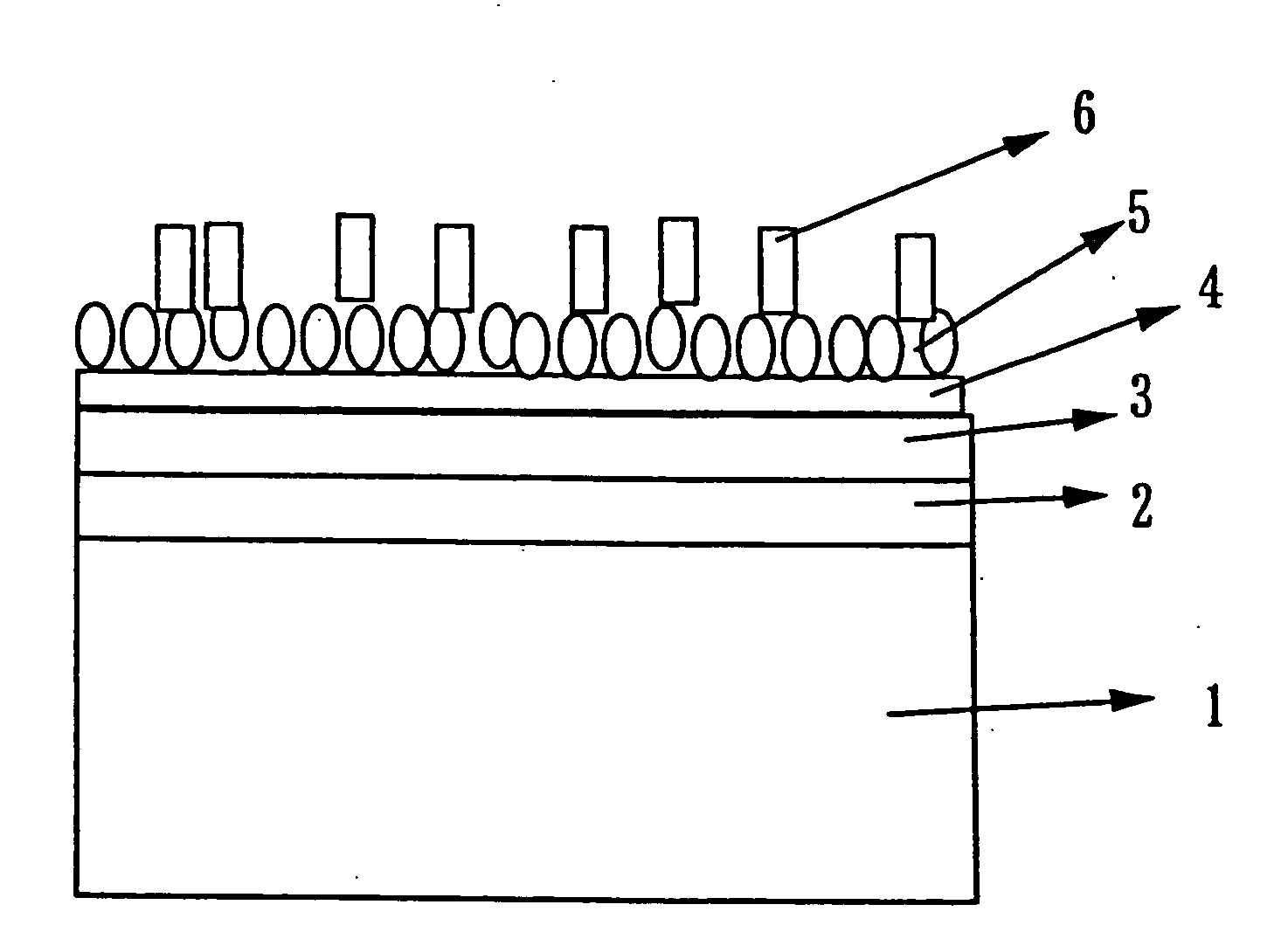
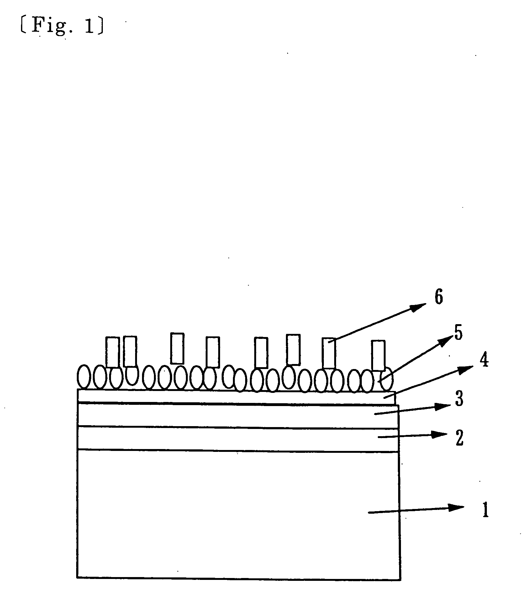
[0085]One example of protein chip according to this invention will be described based on FIG. 1. In this protein chip, a metallic layer 2 is provided on a solid base 1, and a thin film active layer 3 made from a nonmetallic material is provided on the metallic layer 2. A modification layer 4 described later in this specification is formed on a surface portion of the active layer 3. On the modification layer 4, a probe protein 5 capable of adsorbing a test substance 6 (test protein, for example) is immobilized. The protein chip is usable for infrared reflection absorption analysis due to the above-described constitution, which is the great characteristic of the protein chip.

[0086]The form and the size of the solid base are not limited. A material to be used for the solid base may be selected arbitrarily, and preferred examples thereof include Si, SiO2, quartz, and ceramic such as titania.

[0087]A material to be used for the metallic layer is not particularly limited, too, ...

example 1

[0096]Hereinafter, one example of biochip production by a chemical modification method (method for forming a metallic layer and an active layer) particularly contrived by the inventors of this invention will be described.

[0097]In this example,

(1) a metallic layer is formed on a solid base,

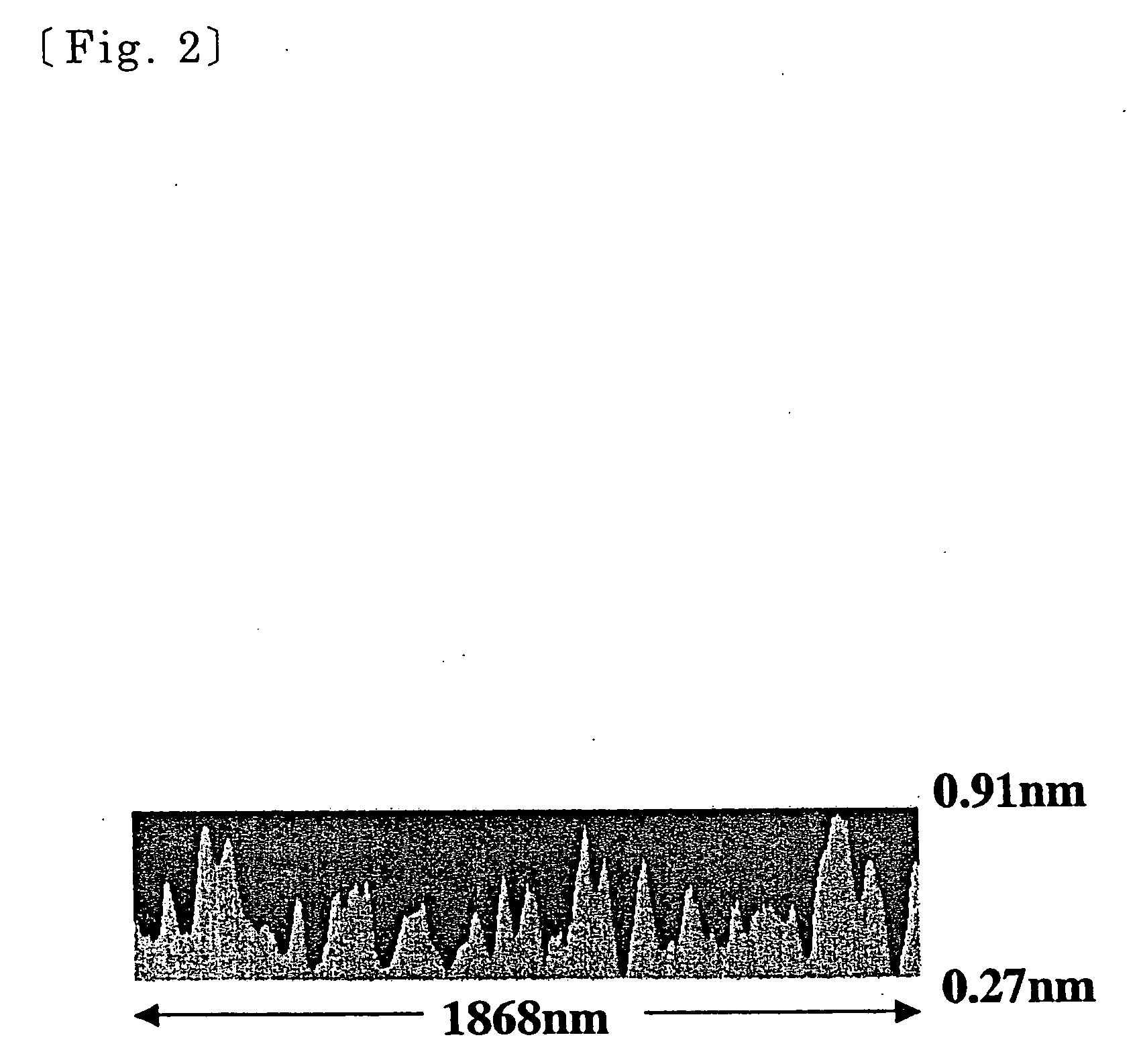
(2) a nonmetallic material is deposited on the metallic layer by vapor deposition, sputtering, or chemical vapor deposition (CVD), and then an active layer made from a nonmetallic material and having a film thickness less than an infrared wavelength and a flatness in terms of difference of elevation of 5 nm or less is formed by annealing, and

(3) a probe is immobilized on a surface of the active layer.

[0098]In immobilizing the probe, it is possible to form a modification layer in which a reaction group such as a carboxyl group, an amino group, and the like is attached to the surface by, for example, reacting a silane coupling agent with the surface of the active layer followed by a hydrolysis reacti...

example 2

[0104]As the carboxylation of the active layer surface described in Example 1, a method formed of a first step and a second step described below is particularly excellent.

[0105]First Step: The chip of Example 1 on which the annealing is performed is dipped into 0.5 mM / L of a toluene solution of carbomethoxyethyltrichlorosilane at −8° C. for one hour. Then, the chip is washed with toluene, acetone, methanol, and pure water in this order.

[0106]Second Step: The chip is dipped into a concentrated hydrochloric acid solution for 3 to 8 hours for hydrolysis.


PUM

PropertyMeasurementUnit
surface flatnessaaaaaaaaaa
temperatureaaaaaaaaaa
thicknessaaaaaaaaaa

Abstract

A biochip to be used for infrared reflection absorption spectroscopy analysis, which is obtainable by forming a metallic layer and an active layer made from a nonmetallic material and has a film thickness less than an infrared wavelength and remarkably flat surface on a solid base and immobilizing a probe on the active layer. A biochip analysis apparatus including the biochip, a liquid passing unit for supplying a sample liquid containing a test substance to the biochip, and an optical system entering infrared light to the biochip and detecting a reflected infrared light. A biochip analysis method using the apparatus.As described above, the novel biochip that is useful for infrared reflection absorption spectroscopy analysis, the biochip analysis apparatus incorporating the biochip, and the biochip analysis method are provided.

Description

BACKGROUND OF THE INVENTION[0001]1. Field of the Invention[0002]This invention relates to a biochip for detecting presence or absence of a test substance in a sample. More specifically, this invention relates to a novel biochip production method, an excellent biochip produced by the method, a biochip analysis apparatus realized by incorporating the biochip, and a biochip analysis method using the biochip analysis apparatus. Representative examples of the “biochip” of this invention include a protein chip, a nucleic acid chip (DNA chip), a cell chip, and the like.[0003]2. Description of the Related Art[0004]As an analysis method of a protein chip, the Surface Plasmon Resonance method (SPR method), the Enzyme-Linked ImmunoSorbent Assay method (ELISA method), and the like have heretofore been known. The protein chip is a chip used for confirming the presence or absence of a test substance reacting with a specific protein. The SPR method is a method for considering a change in physical ...

Claims


Application Information

Patent Timeline
Patent Type & Authority Applications(United States)
IPC IPC(8): G01N21/01C23C16/00C23C14/34B01J19/00C12M1/34C12M1/00C12N15/09C12Q1/02C12Q1/68G01N21/27G01N21/35G01N21/3581G01N21/41G01N21/552G01N21/78G01N33/53G01N33/543G01N33/566G01N37/00
CPCB82Y15/00B82Y30/00G01N21/78G01N33/54393
Inventor URISU, TSUNEOSUZUI, MITSUKAZU
Owner JAPAN SCI & TECH CORP
Why Eureka
Try Eureka