

Optical integrated device and manufacturing method thereof
- Summary
- Abstract
- Description
- Claims
- Application Information
AI Technical Summary
Benefits of technology
Problems solved by technology
Method used
Image

Examples
first embodiment
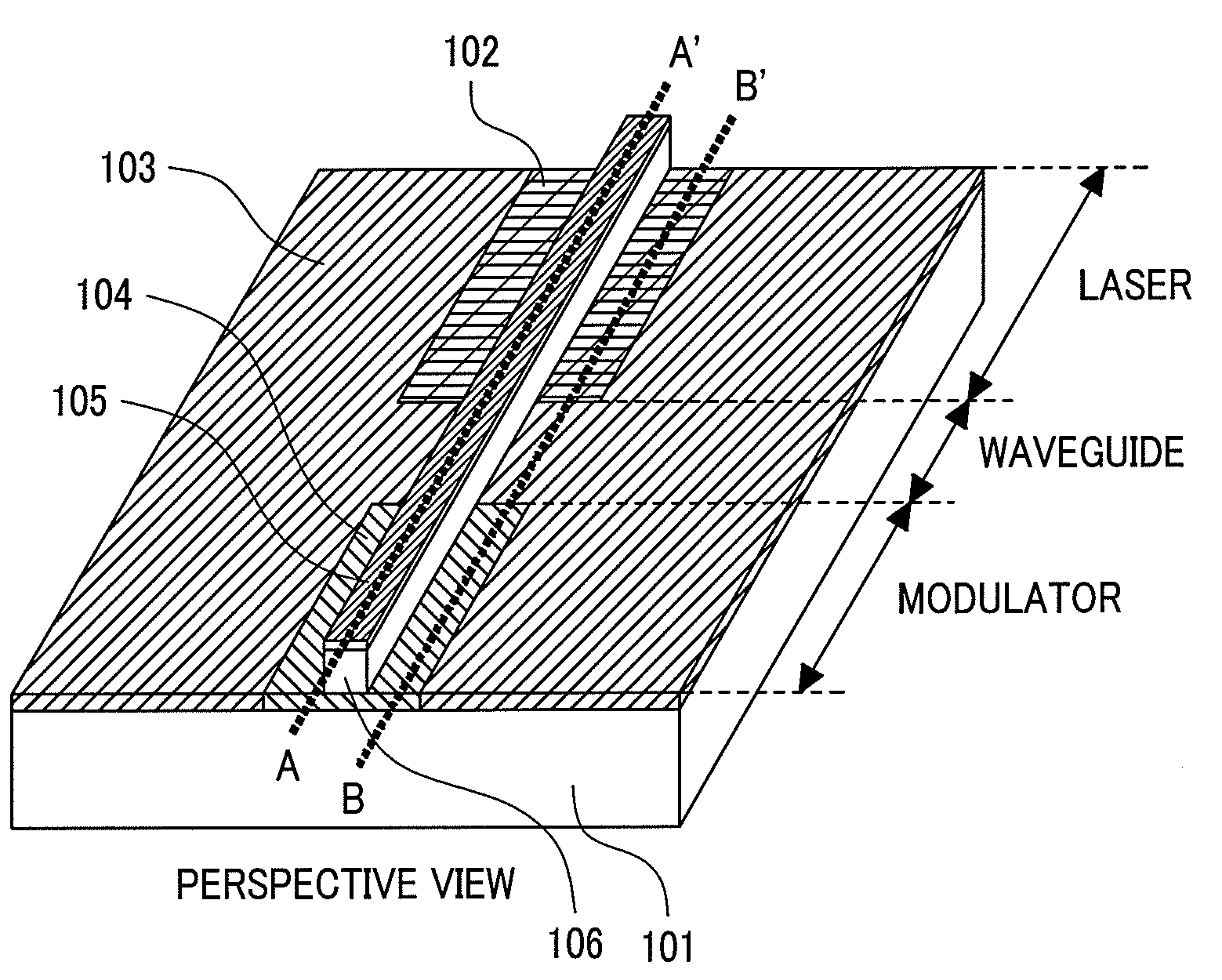
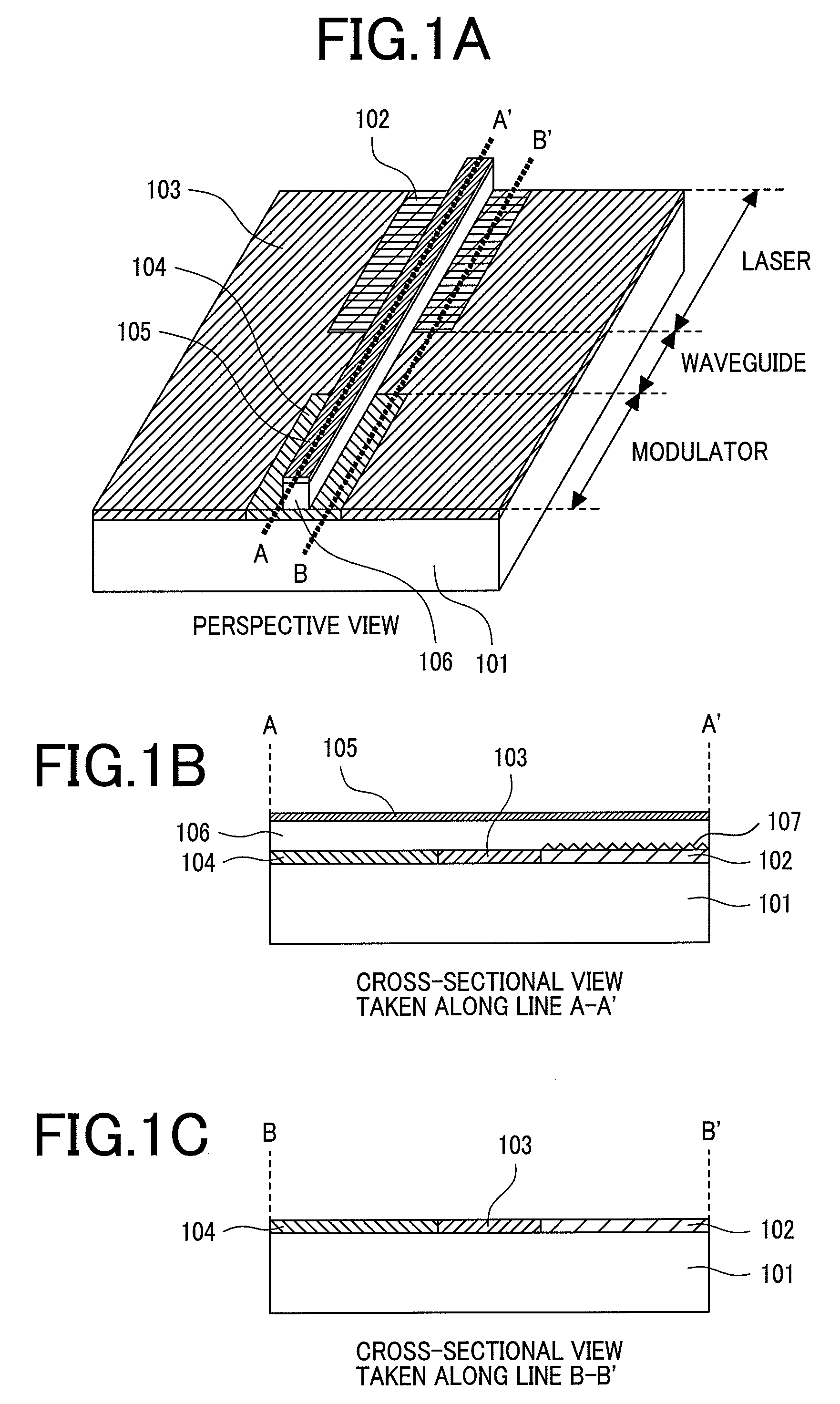
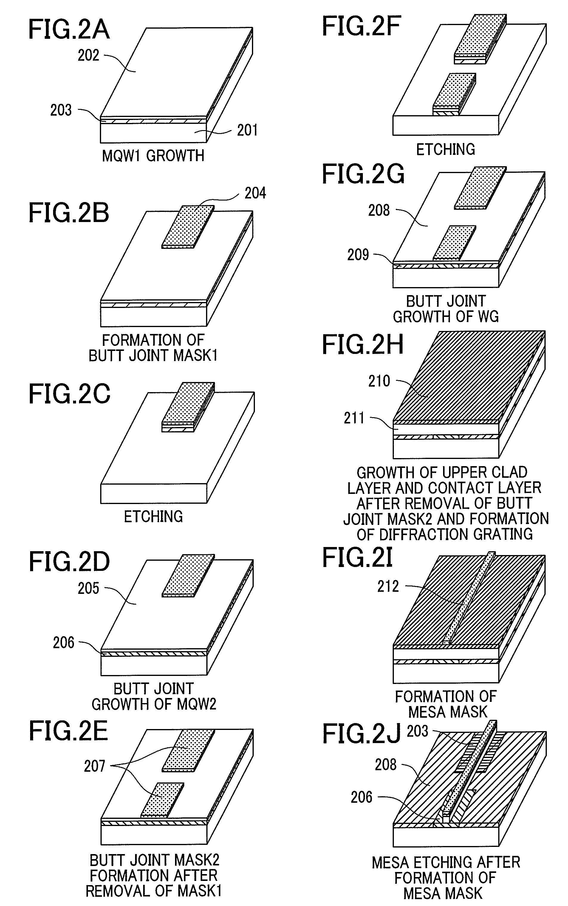
[0050]In a first embodiment of the present invention, the present invention is applied to the modulator-integrated laser with ridge waveguide structured as described above. As the growth method, the metal-organic vapor phase epitaxy (MOVPE) is used. As source materials which supply the group III elements, triethyl garium (TEG), trimethyl indium (TMI), and trimethyl aluminum (TMA) are used. As source materials which supply the group V elements, arsine (AsH3) and phosphine (PH3) are used. As a source material for n-type dopant, disilane (Si2H6) is used, and as a source material for p-type dopant, dimethyl zinc (DMZ) is used. The growth method is not restricted to the MOVPE method, and it is allowable to employ any other method including the molecular beam epitaxy (MBE) method, the chemical beam epitaxy (CBE) method, the metal-organic molecular bean epitaxy (MOMBE) method.
[0051]FIG. 4A is a perspective view of the device. In this figure, a optical window section and electrodes are omit...
second embodiment
[0057]In a second embodiment of the present invention, the present invention is applied to a short cavity Distributed Bragg Reflector (DBR) laser. This laser is novel light source in which a cavity length is extremely short and a high speed operation is possible with a low threshold current as described in the report by Aoki et al, 7p-ZN-18, page 1016 of Collection of 66-th Assembly of Draft Report for Symposium of Applied Physics. The MOVPE method is used as a growth method also in this embodiment, but the growth method is not restricted to the MOVPE method, and any other method may be employed so long as the same effect is provided. The source materials used in the second embodiment are the same as those used in the first embodiment. FIG. 7A is a perspective view of the device. In FIG. 7A, the optical window section and the electrodes are omitted for simplification. The flow of fabricating the device is similar to that in the first embodiment. At first, MQW layer in the laser sect...
third embodiment
[0061]In a third embodiment of the present invention, the present invention is applied to an arrayed optical integrated device. FIG. 8 is a perspective view illustrating the device. In FIG. 8, the optical window section and the electrodes are omitted for simplification. This device is an example of a device in which laser beam emitted from the one laser among four-channel lasers arrayed in parallel and is guided to the modulator section by a optical multiplexer via a waveguide and is modulated by modulator. In FIG. 8, reference numeral 803 denotes an MQW1 ayer in the laser section; and 807, an MQW2 layer in the modulator section. The MQW1 layer in the laser section 803 and the MQW2 layer in the modulator section 807 are connected with an optical multiplexer 808 and a waveguide 810. In the third embodiment, the MOVPE method is employed as a growth method, but the growth method is not restricted to the MOVPE method, and any other method may be employed so long as the same effect can b...
PUM
 Abstract
Description
Claims
Application Information