Organic electroluminescence device and material for organic electroluminescence device

Active Publication Date: 2009-01-08
IDEMITSU KOSAN CO LTD
View PDF19 Cites 56 Cited by
  • Summary
  • Abstract
  • Description
  • Claims
  • Application Information

AI Technical Summary

Benefits of technology

042]According to the aspect of the present invention, by using the host material represented by the formula (1) as the phosphorescent host, a phosphorescent organic EL device having high efficiency and long lifetime can be provided.

Problems solved by technology

However, although an organic EL device in which CBP is used as the host material exhibits much higher luminous efficiency due to phosphorescent emission, the organic EL device has such a short lifetime as to be practically inapplicable.
Such a problem is considered to be attributed to considerable degradation of molecules by holes due to not-high oxidation stability that the molecular structure of CBP exhibits.
Although the technique disclosed in Document 2 contributes to an improvement in the luminous efficiency and lifetime, the improved luminous efficiency and lifetime are not always sufficient for practical application.
Accordingly, it is not successful to simply apply the fluorescent host to the host material (phosphorescent material) for a phosphorescent-emitting layer.
Thus, energy cannot be

Method used


Image

  • Organic electroluminescence device and material for organic electroluminescence device
  • Organic electroluminescence device and material for organic electroluminescence device
  • Organic electroluminescence device and material for organic electroluminescence device

Examples


synthesis example

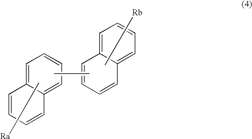
[0303]Compounds according to the present invention can be synthesized by Suzuki-Miyaura cross coupling reaction. For instance, the compounds are synthesized as shown in the following chemical reaction formulae.

(Ra—Ar1—Br)+((OH)2B—Ar2—Rb→Ra—Ar1—Ar2—Rb

((Ra—B(OH)2)+I—Ar1—Br)→(Ra—Ar1—Br))

[0304]Next, a manufacturing method of the host material according to the present invention will be described with reference to synthesis example(s). However, the present invention is not limited to such synthesis examples.

[0305]Under an argon gas atmosphere, 8.0 g (21 mmol) of 2-bromo-6-(9-phenanthryl)naphthalene, 6.2 g (21 mmol) of 3-(9-phenanthryl)phenylboronic acid, 490 mg (0.42 mmol) of tetrakis(triphenylphosphine)palladium(0), 150 mL of toluene, 50 mL of dimethoxyethane and 30 mL of 2M sodium carbonate solution were mixed, and stirred for 12 hours at 90 degrees C. Subsequently, the reaction mixture was cooled down to room temperature, added with water and stirred for one hour. Then, the reaction mi...

example 1

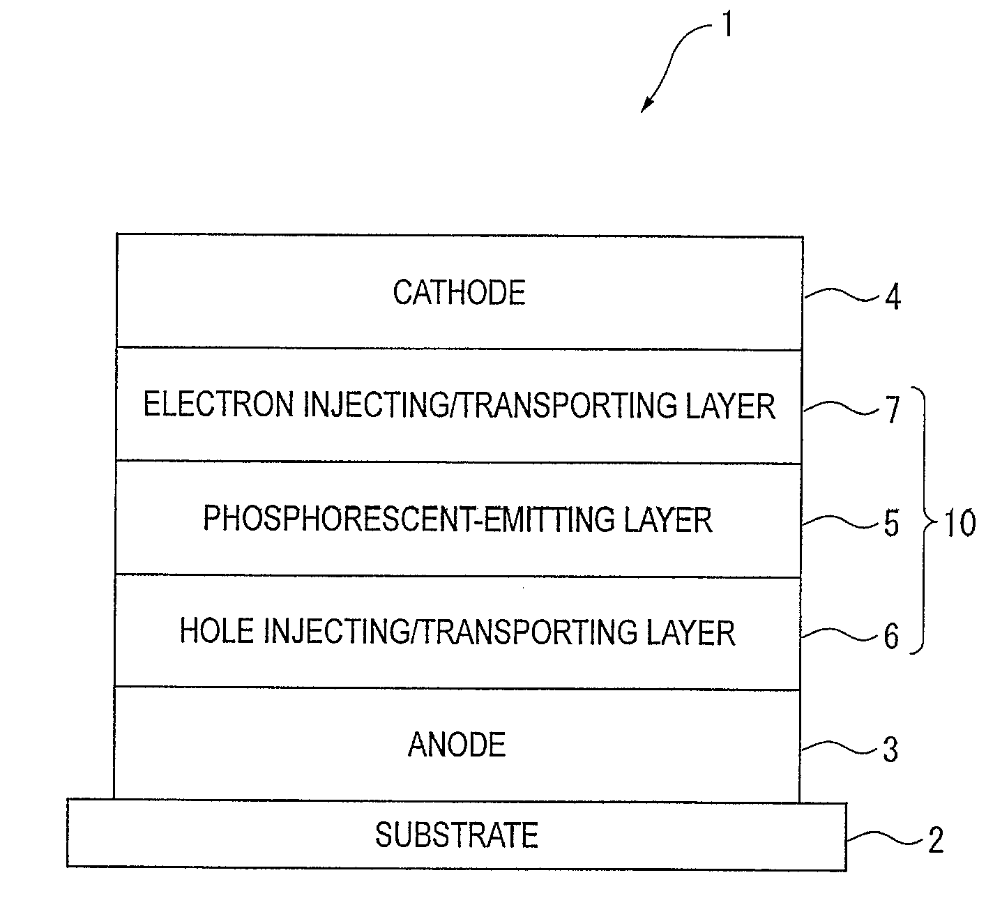
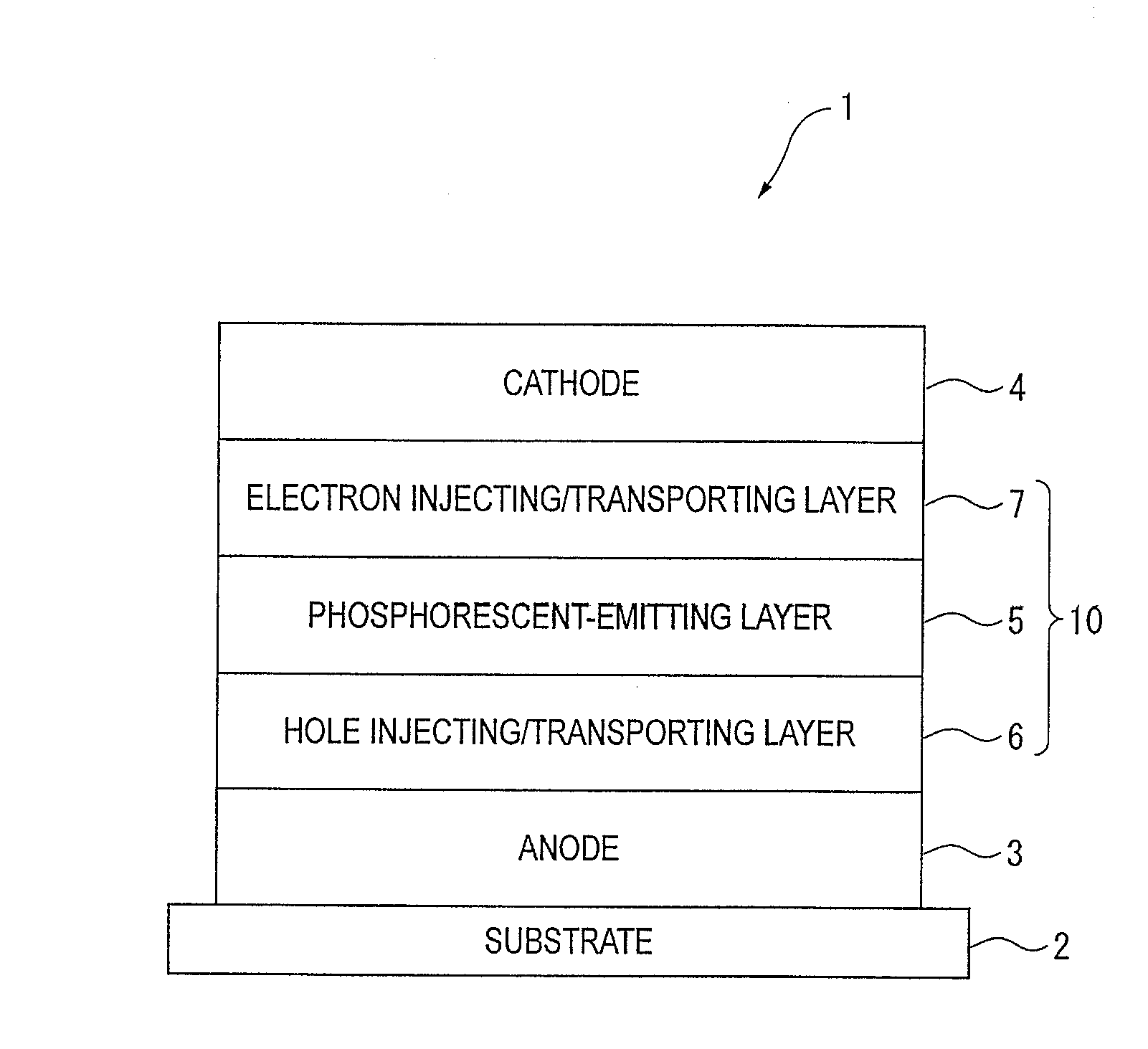
[0330]Manufacturing of Organic EL Device

[0331]A glass substrate (size: 25 mm×75 mm×0.7 mm thick) having an ITO transparent electrode (manufactured by Asahi Glass Co., Ltd) was ultrasonic-cleaned in isopropyl alcohol for five minutes, and then UV / ozone-cleaned for 30 minutes. After the glass substrate having the transparent electrode line was cleaned, the glass substrate was mounted on a vacuum deposition apparatus, so that 50-nm thick film of HT1 was initially formed to cover a surface of the glass substrate where the transparent electrode line was provided. The HT1 film serves as a hole injecting / transporting layer. Subsequently to the formation of the hole injecting / transporting layer, 40-nm thick film of the compound B24 and a film of Ir(piq)3 as a phosphorescent dopant were co-evaporated by resistance heating so that Ir(piq)3 was contained therein with a content of 10 mass %. The co-deposited film serves as an emitting layer (phosphorescent-emitting layer). After the film of the...


PUM

PropertyMeasurementUnit
Wavelengthaaaaaaaaaa
Energyaaaaaaaaaa

Abstract

An organic electroluminescence device includes: a cathode; an anode; and a single-layered or multilayered organic thin-film layer provided between the cathode and the anode. In the organic electroluminescence device, the organic thin-film layer includes at least one emitting layer, and the at least one emitting layer contains: at least one phosphorescent material; and a host material represented by the following formula (1).
Ra—Ar1—Ar2—Rb   (1)
In the formula, Ar1, Ar2, Ra and Rb each represent a substituted or unsubstituted benzene ring or a substituted or unsubstituted condensed aromatic hydrocarbon group selected from a group consisting of a naphthalene ring, a chrysene ring, a fluoranthene ring, a triphenylene ring, a phenanthrene ring, a benzophenanthrene ring, a dibenzophenanthrene ring, a benzotriphenylene ring, a benzochrysene ring, a picene ring and a benzo[b]fluoranthene ring.

Description

BACKGROUND OF THE INVENTION[0001]1. Field of the Invention[0002]The present invention relates to an organic electroluminescence device (hereinafter abbreviated as organic EL device) and a material for organic electroluminescence device. In particular, the present invention relates to an organic electroluminescence device including a red emitting layer and a material used for the organic electroluminescence device.[0003]2. Description of Related Art[0004]An organic EL device, which includes an organic thin-film layer (in which an emitting layer is included) between an anode and a cathode, has been known to emit light using exciton energy generated by a recombination of holes and electrons that have been injected into the emitting layer.[0005]Such an organic EL device, which has the advantages as a self-emitting device, is expected to serve as an emitting device excellent in luminous efficiency, image quality, power consumption and thin design.[0006]An example of a further improvement...

Claims


Application Information

Patent Timeline
IPC IPC(8): H01L51/52C09K11/06
CPCC09K2211/1007C09K2211/1011H05B33/20Y10S428/917H10K85/615H10K85/631H10K85/626H10K85/657H10K85/342H10K85/6572H10K50/11H10K2101/10H10K50/14H10K50/171H10K2102/103
Inventor NISHIMURA, KAZUKIIWAKUMA, TOSHIHIROFUKUOKA, KENICHIHOSOKAWA, CHISHIOKAWAMURA, MASAHIROITO, MITSUNORITAKASHIMA, YORIYUKIOGIWARA, TOSHINARI
Owner IDEMITSU KOSAN CO LTD
Why Eureka
Try Eureka