Ion doping apparatus, ion doping method, semiconductor device and method of fabricating semiconductor device

a technology of ion doping apparatus and semiconductor device, which is applied in the direction of semiconductor/solid-state device testing/measurement, nuclear engineering, therapy, etc., can solve the problems of method presentation of technical difficulty, inferior physical characteristics such as electrical conductivity poor controllability of amorphous silicon semiconductor thin films, etc., to achieve stable doping and good controllability of doping amoun

Inactive Publication Date: 2009-01-15
SHARP KK
View PDF5 Cites 15 Cited by
  • Summary
  • Abstract
  • Description
  • Claims
  • Application Information

AI Technical Summary

Benefits of technology

[0022]In order to overcome such problems of conventional techniques, an objective of the present invention is to provide an ion doping apparatus and ion doping method which provides good contr

Problems solved by technology

However, amorphous silicon semiconductor thin films are inferior in physical characteristics such as electrical conductivity.
Therefore, amorphous silicon semiconductor thin films are not suitable for, for example, the aforementioned devices whose semiconductor elements are required to show excellent performance.
Therefore, this method presents a technical difficulty when forming a crystalline silicon semiconductor thin film having good semiconductor characteristics over the entire surface of a substrate which has a large area.
Moreover, since it is necessary to perform the film formation at a temperature of 600° C. or above, it is impossible to use a glass substrate, which is inexpensive and has a low softening point, as an insulative substrate.
This presents a problem in terms of production cost.
However, it may be difficult to provide a practical means for irradiating intense light over a large area.
For example, in the case of employing an excimer laser (which is a most common choice at present), the stability of laser light is insufficient.
Therefore, it is difficult to obtain a crystalline silicon film by applying a uniform process over the entire face of a substrate which has a large area.
This makes it difficult to form a plurality of semiconductor elements having uniform characteristics on the same substrate.
Moreover, the irradiation area of laser light is small, thus leading to poor production efficiency.
Therefore, if the heat treatment were to be conducted at a lower temperature in order to employ an inexpensive glass substrate, the heating time would have to be increased, which would result in a lower throughp

Method used


Image

  • Ion doping apparatus, ion doping method, semiconductor device and method of fabricating semiconductor device
  • Ion doping apparatus, ion doping method, semiconductor device and method of fabricating semiconductor device
  • Ion doping apparatus, ion doping method, semiconductor device and method of fabricating semiconductor device

Examples


Embodiment Construction

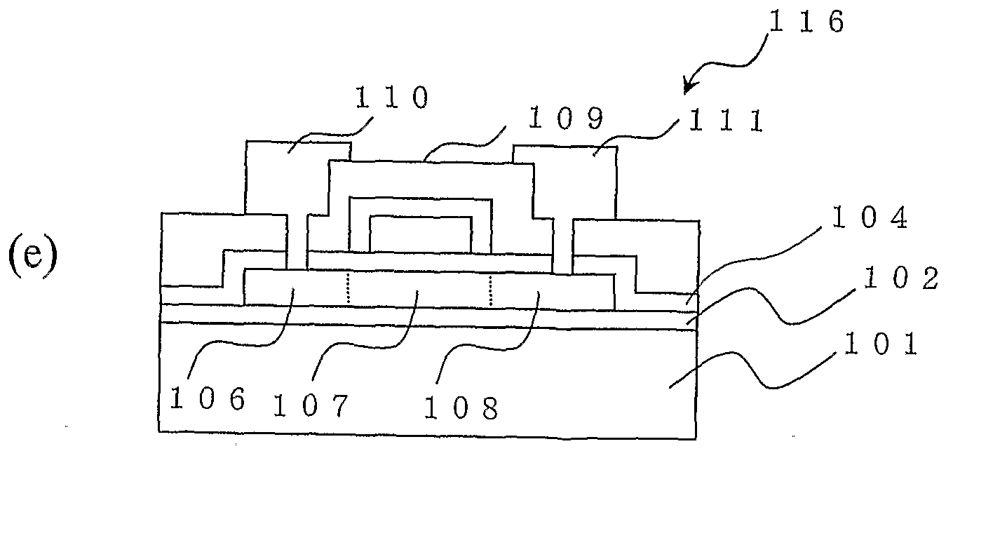
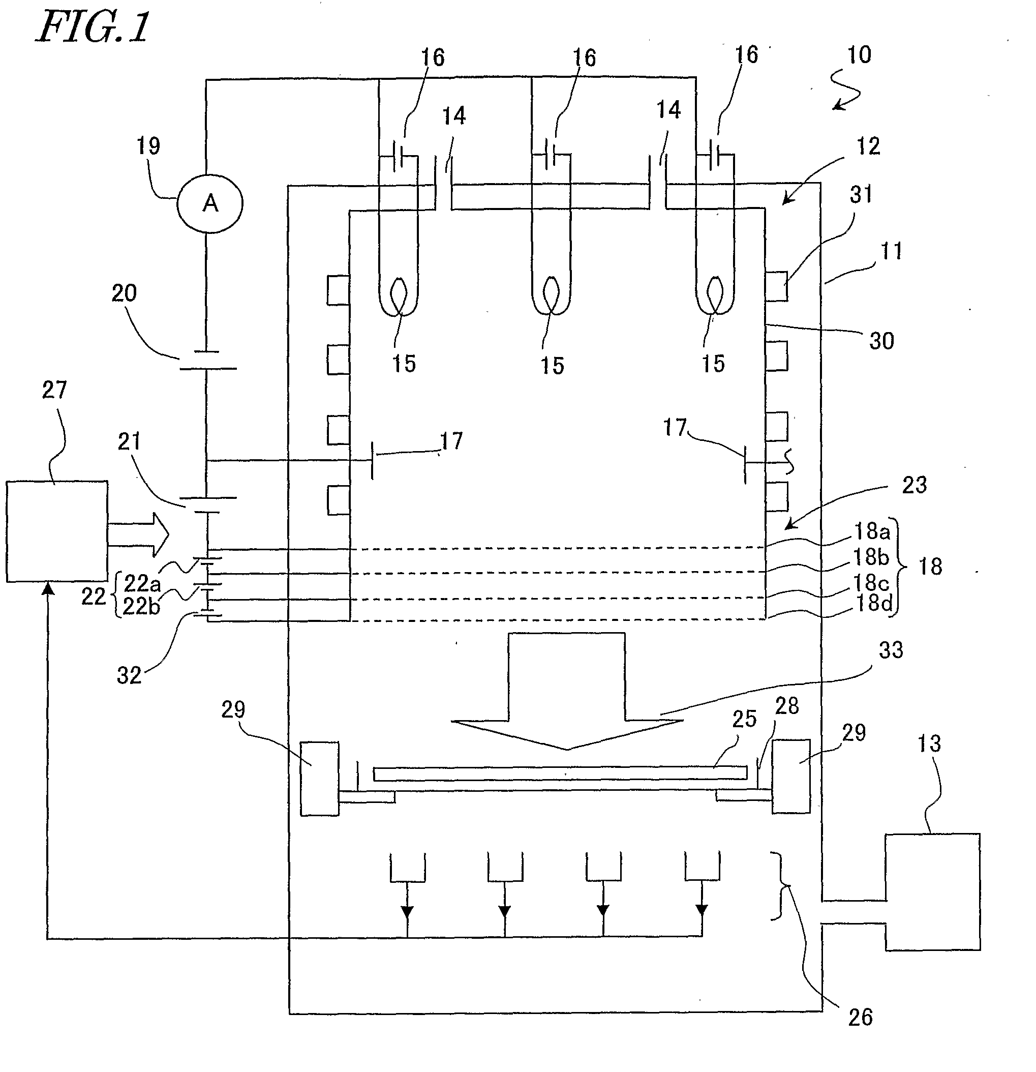
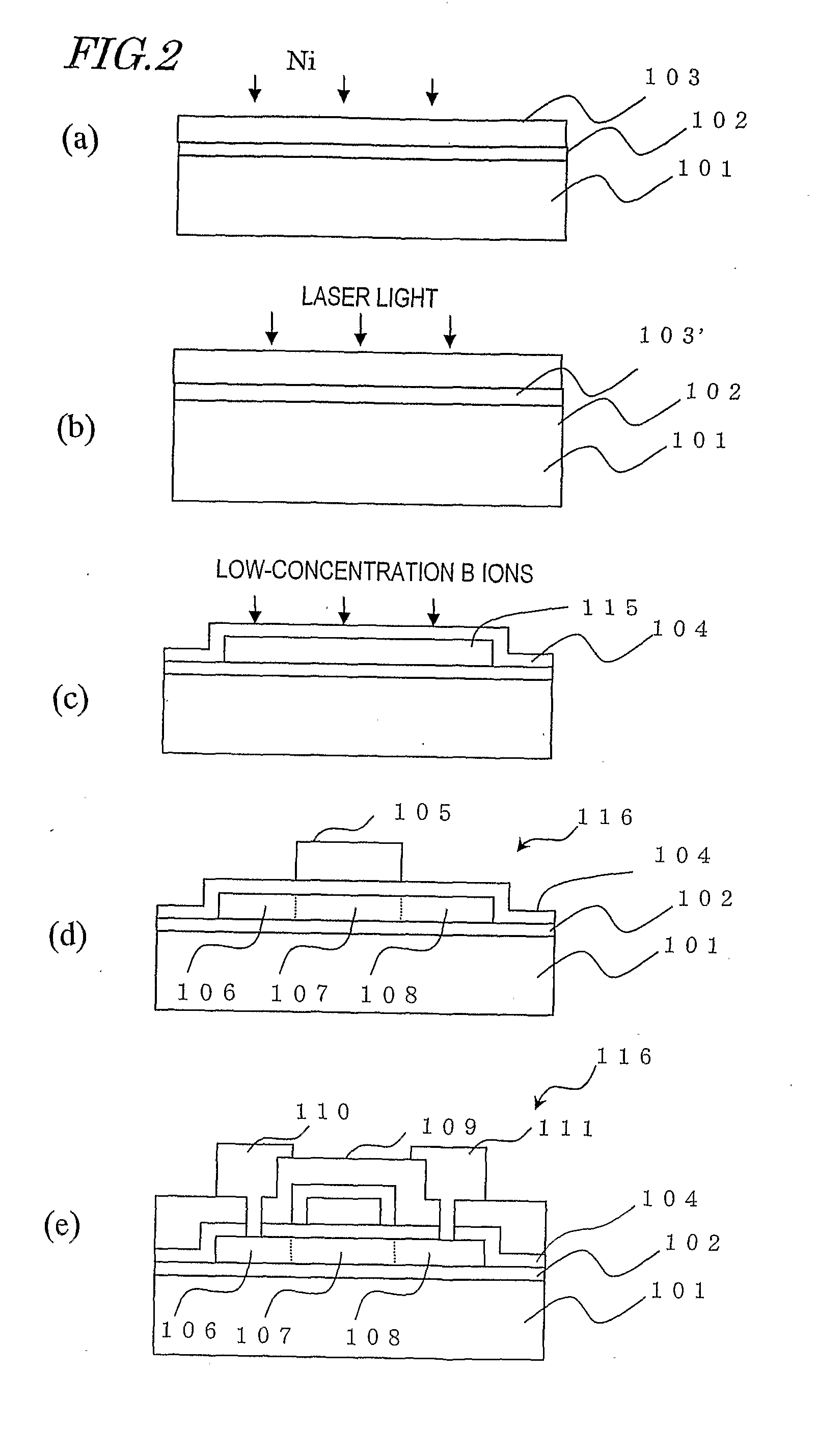
[0050]FIG. 1 shows an embodiment of an ion doping apparatus of the present invention. The ion doping apparatus 10 shown in FIG. 1 comprises a chamber 11, a discharge section 13, an ion source 12, an acceleration section 23, and a control section 27.

[0051]The discharge section 13, which may be composed of a known pump or the like, discharges the gaseous content from within the chamber 11 so as to maintain the pressure within the chamber at an appropriate value. Although not shown, the discharge section 13 is connected to a detoxification apparatus for detoxifying various gases which may be used in the ion doping apparatus.

[0052]The ion source 12 generates plasma by decomposing a gas which contains elements to be used for doping through, for example, arc discharge, thus generating ions containing an element(s) to be used for doping. The ion source 12, which is provided in the chamber 11, includes an arc chamber 30, gas inlets 14, and filaments 15. The gas inlets 14 are provided in the...


PUM


Abstract

An ion doping apparatus includes: a chamber 11; a discharge section 13 for discharging a gaseous content from within the chamber 11; an ion source 12 being provided in the chamber 11 and including an inlet 14 through which to introduce a gas containing an element to be used for doping, the ion source 12 decomposing the gas introduced through the inlet 14 to generate ions containing the element to be used for doping; an acceleration section 23 for pulling out from the ion source 12 the ions generated at the ion source 12 and accelerating the ions toward a target object held in the chamber; and a beam current meter 26 for measuring a beam current caused by the accelerated ions. The beam current is measured by the beam current meter 26 a plurality of times, and if a result of the measurements indicates a stability of the beam current, the ion doping apparatus automatically begins to implant into the target object the ions containing the element to be used for doping. Thus, an ion doping apparatus having excellent doping amount controllability is provided.

Description

TECHNICAL FIELD[0001]The present invention relates to an ion doping apparatus for performing an ion implantation or doping for a target object, and more particularly to an ion doping apparatus which provides good mass producibility. The present invention also relates to a semiconductor device which is fabricated by using an ion doping apparatus.BACKGROUND ART[0002]In recent years, with a view to producing large-sized and high-resolution liquid crystal display devices, fast and high-resolution image sensors of a close-contact type, three-dimensional ICs and the like, attempts have been made at forming a high-performance semiconductor element on an insulative substrate such as glass.[0003]In order to form such a semiconductor element, it is necessary to form a thin-film layer of semiconductor. It has been known to form a semiconductor element on an insulative substrate by using a semiconductor thin film composed of an amorphous silicon semiconductor (a-Si) or using a semiconductor thi...

Claims


Application Information

Patent Timeline
IPC IPC(8): H01L29/04H01L21/66H01J37/08H01J37/304H01L21/00H01L21/336H01L29/786
CPCH01J37/304H01J2237/0815H01L29/78675H01L21/67115H01L29/66757H01J2237/31701
Inventor NAKANISHI, KEN
Owner SHARP KK
Why Eureka
Try Eureka