Magnetic reading head and magnetic recording apparatus

a reading head and magnetic recording technology, applied in the manufacture of flux-sensitive heads, instruments, record information storage, etc., can solve the problems of unstable magnetic material magnetization in each of the existing cpp-gmr heads and tmr heads, difficult to maintain magnetization, and increase magnetic noise, so as to reduce the volume of a free layer, suppress the increase of magnetic noise, and reduce electrical noise

a reading head and magnetic recording technology, applied in the manufacture of flux-sensitive heads, instruments, record information storage, etc., can solve the problems of unstable magnetic material magnetization in each of the existing cpp-gmr heads and tmr heads, difficult to maintain magnetization, and increase magnetic noise, so as to reduce the volume of a free layer, suppress the increase of magnetic noise, and reduce electrical noise

US20090034131A1Inactive Publication Date: 2009-02-05HITACHI LTD

Image

  • Magnetic reading head and magnetic recording apparatus
  • Magnetic reading head and magnetic recording apparatus
  • Magnetic reading head and magnetic recording apparatus

Examples


example 1

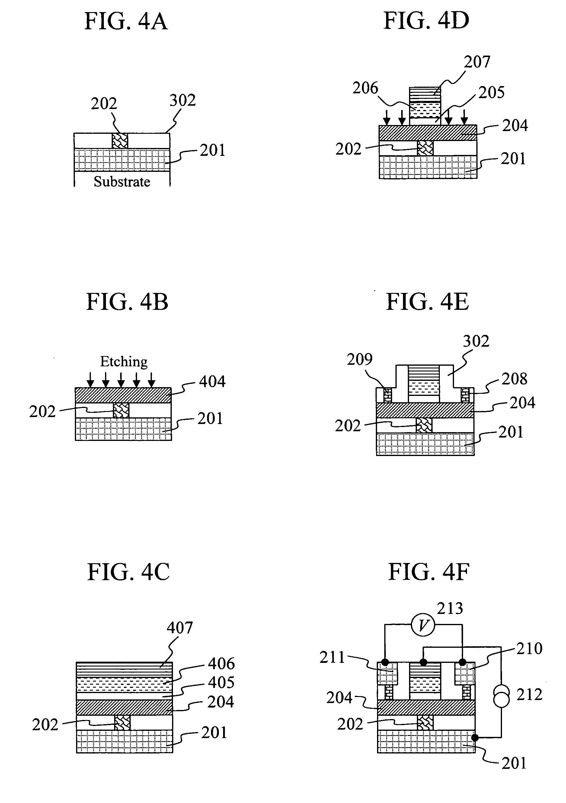
[0060]A magnetic reading head including the second modulated spin accumulation device by magnetic field as shown in FIG. 2 was manufactured through the steps shown in FIGS. 4A to 4F. As a substrate, prepared was a commonly-used substrate on which a shield layer was formed. The commonly-used substrate was a SiO2 substrate or a glass substrate (or was a magnesium oxide substrate, a GaAs substrate, an AlTiC substrate, a SiC substrate, an Al2O3 substrate or the like, instead). The shield layer was formed with a film forming apparatus using an RF sputtering method, a DC sputtering method, a molecular beam epitaxy method (MBE) or the like. For example, in the case where an RF sputtering method is employed for forming the shield layer, a predetermined film is caused to grow in an Ar atmosphere under conditions where a pressure is on the order of 0.1 to 0.001 Pa, and a power is 100 W to 500 W. As a substrate on which the device was to be formed, used was either one of the above substrates w...

example 2

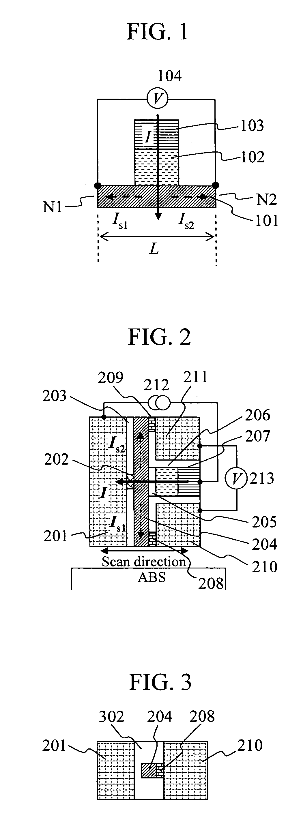
[0068]A magnetic reading head including the third modulated spin accumulation device by magnetic field (refer to FIG. 5) according to the present invention was manufactured through the steps shown in FIGS. 8A to 8F. The following steps 1 to 6 correspond to FIGS. 8A to 8F, respectively.

Step 1: Forming a Pinned Layer (Magnetic Material)

[0069]As an electrode, a Pt film was formed in a thickness of 100 nm on a Si substrate of 3 inches provided with a thermal oxide film using an RF magnetron sputtering apparatus. On the Pt electrode, a MnIr film with a thickness of 10 nm to serve as an antiferro magnetic material, a CoFeB film with a thickness of 4 nm to serve as a pinned layer were sequentially formed. Then, an MgO film with a thickness of 2 nm to serve as a barrier layer was formed on the CoFeB film. Thereafter, as a pattern for the pinned layer, a square pattern of 1×1 μm2 was transferred onto the barrier layer with an I-line stepper, and the thus-formed layers were patterned by ion m...


PUM

PropertyMeasurementUnit
gap widthaaaaaaaaaa
total thicknessaaaaaaaaaa
pressureaaaaaaaaaa

Abstract

To provide a magnetic reading head that features high resolution and low noise, and that can support a hard disk with terabit-level surface recording density. A current is caused to flow from a pinned layer with its magnetization direction fixed by an antiferro magnetic material, to a non-magnetic thin wire having a portion affected by an external magnetic field and a portion not affected by the external magnetic field, so that spin polarized electrons are accumulated in the non-magnetic thin wire. A distance between voltage terminals of a voltmeter is set to less than the spin diffusion length of the non-magnetic thin wire. A change in the external magnetic field modulates some of the accumulated spin polarized electron, but does not others. Accordingly, an electrical potential difference depending on the external magnetic field is generated between the both end surfaces of the non-magnetic thin wire, and measured with the voltmeter.

Description

CLAIM OF PRIORITY[0001]The present application claims priority from Japanese application JP 2007-202224 filed on Aug. 2, 2007, the content of which is hereby incorporated by reference into this application.BACKGROUND OF THE INVENTION[0002]1. Field of the Invention[0003]The present invention relates to a magnetic reading head including a magnetoresistance effect device and a magnetic recording apparatus equipped with the magnetic reading head.[0004]2. Description of the Related Art[0005]Heretofore, magnetic recording and reproducing apparatuses have been improved in recording density at a rate of more than 40% a year, and it is estimated that the recording density will reach the order of Tbit / in2 around the year of 2011 at the present rate of growth. Such a terabit-level magnetic recording apparatus needs to be equipped with a magnetic writing and reading head with higher output and higher resolution than ever.[0006]As an elemental technique for an existing magnetic recording and rep...

Claims


Application Information

Patent Timeline
05 Feb 2009
Publication
US20090034131A1
IPC
G11B5/33
CPC
B82Y25/00; G01R33/093; H01L43/08; G11B5/3903; G01R33/1284; H10N50/10
Inventors
YAMADA, MASAKI; TAKAHASHI, HIROMASA